

What Are the Advances in OLED vs MicroLED Circuitry Design
OCT 24, 20259 MIN READ
Generate Your Research Report Instantly with AI Agent
PatSnap Eureka helps you evaluate technical feasibility & market potential.
OLED and MicroLED Display Technology Evolution
The evolution of display technologies has witnessed significant advancements over the past decades, with OLED (Organic Light-Emitting Diode) and MicroLED emerging as frontrunners in next-generation display solutions. OLED technology, first conceptualized in the 1970s and commercialized in the late 1990s, revolutionized displays with its self-emissive properties, eliminating the need for backlighting and enabling thinner, more flexible screens with superior contrast ratios.
The technological trajectory of OLED has progressed through several critical phases. Initially, passive-matrix OLED (PMOLED) displays dominated the market, suitable primarily for small screens with limited resolution. The subsequent development of active-matrix OLED (AMOLED) technology in the early 2000s marked a significant breakthrough, incorporating thin-film transistors (TFTs) that enabled independent pixel control, higher resolution, and improved power efficiency.
MicroLED technology represents a more recent innovation, emerging in the mid-2000s as a potential successor to OLED. Unlike OLED's organic compounds, MicroLED utilizes inorganic gallium nitride (GaN) materials to create microscopic LED arrays. This fundamental material difference has profound implications for display performance, longevity, and manufacturing processes.
The circuitry design evolution for both technologies has followed distinct paths. OLED circuitry has evolved from simple passive matrix arrangements to sophisticated active matrix designs incorporating low-temperature polysilicon (LTPS) and indium gallium zinc oxide (IGZO) TFT backplanes. Recent innovations include top-emission structures and tandem OLED architectures that have significantly enhanced efficiency and lifespan.
MicroLED circuitry design, meanwhile, has focused on overcoming unique challenges related to miniaturization and mass transfer processes. The development of advanced driver ICs capable of delivering precise current to microscopic LED elements represents a critical advancement. Additionally, innovative approaches to pixel addressing and current compensation have emerged to ensure uniformity across the display.
Both technologies have seen parallel advancements in flexible and transparent display capabilities, though through different technical approaches. OLED has leveraged its inherent flexibility through the development of plastic substrates and encapsulation technologies, while MicroLED research has explored novel transfer techniques and interconnect structures to achieve similar form factors.
The most recent technological milestone has been the development of hybrid approaches that combine elements of both technologies, such as quantum dot-enhanced MicroLEDs and color-converted MicroLED displays, which aim to leverage the strengths of each technology while mitigating their respective limitations.
Market Demand Analysis for Advanced Display Technologies
The display technology market is witnessing unprecedented growth driven by consumer electronics, automotive interfaces, and emerging applications in augmented and virtual reality. Current market analysis indicates that the global advanced display market is projected to reach $167 billion by 2025, with OLED technology currently dominating premium segments while MicroLED emerges as a promising contender. This dynamic creates significant opportunities for circuitry design innovations across both technologies.
Consumer demand for thinner, more energy-efficient displays with superior image quality continues to intensify. Smartphone manufacturers report that display quality ranks among the top three purchase decision factors for premium devices, creating strong market pull for advanced circuitry solutions that enable better pixel density, refresh rates, and power management. The automotive sector represents another rapidly expanding market, with premium vehicles increasingly featuring multiple display panels requiring specialized circuitry to withstand environmental stresses.
OLED displays currently command approximately 30% of the smartphone display market by value, with annual growth rates exceeding 15% in premium segments. However, industry surveys indicate growing consumer awareness of burn-in issues and limited lifespan, creating market openings for MicroLED alternatives. Commercial adoption of MicroLED remains limited by manufacturing costs, but market forecasts suggest rapid expansion once price points become competitive.
The enterprise and professional display sectors demonstrate increasing willingness to invest in advanced display technologies, particularly for applications requiring high brightness, color accuracy, and longevity. This segment values the superior power efficiency promised by next-generation circuitry designs, with energy consumption emerging as a critical decision factor for large-scale deployments.
Regional analysis reveals that East Asian markets lead in early adoption of novel display technologies, followed by North America and Europe. Chinese manufacturers are rapidly expanding production capacity for both OLED and MicroLED, suggesting intensifying competition and potential price pressures that may accelerate market penetration of these technologies.
Supply chain considerations significantly impact market dynamics, with specialized circuitry components often representing production bottlenecks. Industry reports highlight that advanced driver ICs and backplane technologies frequently constrain manufacturing scale-up, creating premium opportunities for innovative circuit design solutions that simplify production processes.
Market research indicates that consumers increasingly prioritize display quality over marginal improvements in other device specifications, suggesting strong revenue potential for breakthrough circuitry designs that enable visible performance advantages in either OLED or MicroLED implementations. This trend appears particularly pronounced in gaming, content creation, and professional visualization applications where display performance directly impacts user experience.
Technical Challenges in OLED vs MicroLED Circuit Design
The development of display technologies has witnessed significant advancements in recent years, with OLED and MicroLED emerging as leading contenders for next-generation displays. However, both technologies face distinct technical challenges in their circuit design that impact their performance, efficiency, and commercial viability.
OLED circuit design confronts several fundamental challenges. The non-uniform aging of organic materials leads to inconsistent current flow across pixels, requiring complex compensation circuits to maintain image quality over time. Thin-film transistor (TFT) backplanes used in OLED displays exhibit threshold voltage shifts during operation, necessitating additional circuitry to stabilize performance. Furthermore, the current-driven nature of OLEDs demands precise current control mechanisms, significantly increasing circuit complexity compared to voltage-driven technologies.
Power efficiency remains a critical challenge for OLED circuitry, particularly for mobile applications. The voltage drop across OLED pixels requires higher driving voltages, leading to increased power consumption. This issue is exacerbated in high-brightness applications, where circuit designers must balance power efficiency against display performance. Additionally, OLED's sensitivity to oxygen and moisture necessitates robust encapsulation solutions, adding another layer of complexity to the overall circuit design.
MicroLED technology presents a different set of circuit design challenges. The primary obstacle lies in the miniaturization of LED chips to microscopic dimensions while maintaining manufacturing yield and performance. The extremely small size of MicroLEDs (typically <50 μm) makes traditional circuit integration approaches inadequate, requiring novel interconnection technologies and driving schemes.
Mass transfer of millions of tiny MicroLED chips onto circuit substrates presents unprecedented manufacturing challenges. Current approaches include pick-and-place methods, laser transfer, and fluid assembly, each with significant limitations in throughput and precision. The yield management becomes exponentially more complex as display resolution increases, with a single defective pixel potentially rendering an entire display unusable.
Thermal management represents another significant challenge for MicroLED circuit design. Despite higher efficiency than OLEDs, the concentrated nature of MicroLED light emission generates localized heat that must be effectively dissipated to prevent performance degradation and ensure longevity. This necessitates innovative thermal management solutions integrated directly into the circuit design.
Both technologies face common challenges in achieving high-resolution displays. As pixel densities increase, the available area for driving circuitry decreases dramatically, pushing the boundaries of semiconductor manufacturing capabilities. This spatial constraint forces engineers to develop increasingly sophisticated circuit architectures that can deliver precise current control within extremely limited physical dimensions.
The pursuit of flexible and foldable displays introduces additional complexities for both technologies, requiring circuit designs that can withstand mechanical stress while maintaining electrical performance. This challenge is particularly acute for MicroLED, where rigid interconnections between microscopic components must somehow accommodate physical deformation.
Current Circuit Design Solutions for OLED and MicroLED
01 OLED and MicroLED Driver Circuit Design
Driver circuits for OLED and MicroLED displays require specialized designs to control pixel illumination with precision. These circuits manage current delivery to individual pixels, ensuring uniform brightness and color accuracy across the display. Advanced driver architectures incorporate features like current compensation, voltage regulation, and timing control to enhance display performance while minimizing power consumption.- OLED and MicroLED Driver Circuit Design: Driver circuits for OLED and MicroLED displays require specialized designs to control pixel illumination with precision. These circuits manage current delivery to individual pixels, ensuring uniform brightness and color accuracy across the display. Advanced driver designs incorporate features like current compensation, voltage regulation, and timing control to enhance display performance and energy efficiency.
- Integration of Control Systems for Display Technologies: Control systems for OLED and MicroLED displays integrate various components including signal processors, timing controllers, and power management units. These systems coordinate the operation of multiple circuit elements to ensure proper display functionality. The integration approaches focus on minimizing signal interference, reducing power consumption, and enabling high refresh rates required for modern display applications.
- Testing and Verification Methodologies for Display Circuits: Testing methodologies for OLED and MicroLED circuitry involve specialized techniques to verify functionality and performance. These approaches include automated test pattern generation, fault simulation, and built-in self-test mechanisms. Verification processes ensure that display circuits meet specifications for brightness control, color accuracy, and response time while identifying potential failure modes before mass production.
- Power Management and Efficiency Optimization: Power management circuits for OLED and MicroLED displays focus on optimizing energy consumption while maintaining display quality. These designs incorporate voltage regulators, current limiters, and power-saving modes that adjust brightness based on content and ambient conditions. Advanced power management techniques include dynamic voltage scaling and selective pixel activation to extend battery life in portable devices.
- Circuit Design Automation and Simulation Tools: Design automation tools and simulation environments specifically tailored for OLED and MicroLED circuitry enable efficient development and optimization. These tools provide capabilities for circuit modeling, performance prediction, and layout optimization. Simulation frameworks allow designers to evaluate thermal characteristics, power consumption, and signal integrity before physical implementation, reducing development cycles and improving reliability.
02 Integration and Miniaturization Techniques for Display Circuitry
Miniaturization techniques for OLED and MicroLED circuitry focus on reducing component size while maintaining functionality. These approaches include advanced semiconductor fabrication methods, system-on-chip integration, and novel interconnect technologies. Integrated circuit designs combine multiple functions into single chips, enabling thinner displays with improved performance characteristics and reduced manufacturing complexity.Expand Specific Solutions03 Power Management and Efficiency Optimization
Power management circuits for OLED and MicroLED displays are designed to optimize energy efficiency while maintaining display quality. These circuits incorporate voltage regulation, current limiting, and adaptive brightness control to reduce power consumption. Advanced designs include power-saving modes, dynamic voltage scaling, and intelligent power distribution systems that respond to content and ambient conditions.Expand Specific Solutions04 Testing and Verification Methodologies for Display Circuits
Testing methodologies for OLED and MicroLED circuitry involve specialized techniques to verify functionality, performance, and reliability. These approaches include automated test pattern generation, built-in self-test circuits, and fault simulation. Advanced verification systems can detect pixel defects, timing issues, and power anomalies before final assembly, improving manufacturing yield and product quality.Expand Specific Solutions05 Circuit Design Automation and Simulation Tools
Design automation tools for OLED and MicroLED circuitry enable efficient development of complex display systems. These tools include specialized simulation software, circuit modeling frameworks, and automated layout generators. Advanced platforms support multi-physics simulation to analyze electrical, thermal, and optical characteristics simultaneously, allowing designers to optimize performance before physical prototyping.Expand Specific Solutions
Key Industry Players in Advanced Display Manufacturing
The OLED vs MicroLED circuitry design landscape is currently in a transitional phase, with OLED technology reaching maturity while MicroLED remains in early commercialization stages. The global market for these advanced display technologies is projected to exceed $200 billion by 2025, driven by demand for higher performance displays in consumer electronics and automotive applications. Leading OLED players like Samsung Electronics, Universal Display Corporation, and BOE Technology have established robust manufacturing ecosystems, while MicroLED development is being pioneered by companies including Chengdu Vistar Optoelectronics and Apple. The competitive dynamics are shifting as traditional OLED manufacturers like LG Display and Japan Display face increasing pressure from Chinese firms like TCL China Star Optoelectronics, which are rapidly advancing their technical capabilities in both technologies through significant R&D investments.
BOE Technology Group Co., Ltd.
Technical Solution: BOE has developed advanced circuitry solutions for both OLED and MicroLED displays. For OLED, BOE utilizes low-temperature polysilicon (LTPS) and oxide TFT backplanes with proprietary compensation circuits that address threshold voltage shifts and mobility variations. Their flexible OLED circuit design incorporates specialized interconnect structures that maintain electrical performance under mechanical stress, achieving bend radii below 1mm. BOE's recent innovation includes a hybrid LTPS-Oxide TFT architecture that combines the high mobility of LTPS with the uniformity of oxide semiconductors. For MicroLED, BOE has developed an active matrix circuit design with integrated drivers that precisely control current to each microLED pixel, crucial for color uniformity. Their circuit architecture incorporates redundancy schemes to improve yield and reliability. BOE has also pioneered a unique mass transfer process for microLED chips with specialized temporary bonding circuits that enable placement accuracy within 2 micrometers while maintaining high throughput.
Strengths: Massive production capacity with multiple advanced fabrication facilities; strong vertical integration from backplane to module assembly; government backing for technology development. Weaknesses: Still catching up to Samsung and LG in highest-end OLED circuit performance; microLED mass production capabilities still in development phase; higher defect rates in complex circuit implementations compared to industry leaders.
Universal Display Corp.
Technical Solution: Universal Display Corporation (UDC) has made breakthrough advancements in OLED circuitry through their proprietary phosphorescent OLED (PHOLED) technology, which achieves nearly 100% internal quantum efficiency compared to 25% for conventional fluorescent OLEDs. Their circuit designs incorporate specialized thin-film transistor (TFT) architectures optimized for their PHOLED materials, enabling lower power consumption while maintaining brightness. UDC has developed novel pixel circuit designs that compensate for TFT threshold voltage variations and OLED degradation, extending display lifetime. Their recent innovations include RGBW pixel circuit arrangements that reduce power consumption by up to 50% for high-brightness applications. For flexible displays, UDC has pioneered specialized circuit designs with stress-resistant interconnects that maintain performance integrity even after thousands of folding cycles. Their latest advancements include transparent OLED circuit designs with specialized electrode materials achieving over 80% transparency while maintaining electrical performance.
Strengths: Industry-leading PHOLED materials with highest efficiency; extensive IP portfolio with over 5,000 issued and pending patents; specialized expertise in OLED materials-circuit integration. Weaknesses: Limited involvement in MicroLED technology; heavy reliance on manufacturing partners for implementation; circuit designs must be adapted by display manufacturers to their specific production processes.
Breakthrough Patents in Display Driving Circuitry
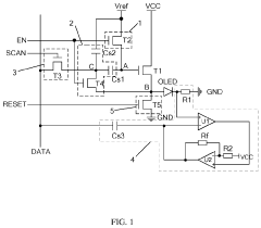
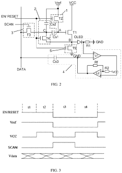
Pixel circuit, driving method thereof and display device
PatentActiveUS20210142728A1
Innovation
- A pixel circuit incorporating a switching sub-circuit, threshold voltage extraction sub-circuit, initialization sub-circuit, feedback compensation sub-circuit, and driving transistor, where the feedback compensation sub-circuit generates data voltage compensation signals based on the operating current of the light emitting device to adjust for threshold voltage shifts and improve display uniformity.
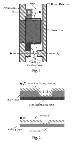
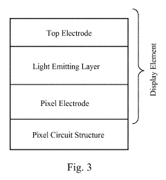
Pixel circuit structure and display device using the same
PatentActiveUS20190288056A1
Innovation
- A pixel circuit structure is designed with a metal light shielding layer electrically coupled to both the power line and display data line through via-holes, reducing resistance and IR drops while increasing storage capacitance, allowing for stable current control without additional metal layers or process changes.
Power Efficiency Comparison and Optimization Strategies
Power efficiency represents a critical differentiator between OLED and MicroLED technologies, with significant implications for device design, battery life, and environmental impact. OLED displays currently demonstrate superior power efficiency in dark-content scenarios due to their self-emissive nature, where black pixels consume virtually no power. This pixel-level power management gives OLED an advantage in applications with predominantly dark interfaces or content.
MicroLED technology, while still maturing, shows promising efficiency characteristics that may eventually surpass OLED capabilities. The theoretical maximum efficiency of MicroLED is higher, particularly at peak brightness levels where OLEDs typically require exponentially more power. Recent advancements in MicroLED driver circuitry have reduced power consumption by implementing sophisticated pulse-width modulation techniques and dynamic refresh rate adjustments.
Both technologies benefit from optimization strategies targeting different aspects of display operation. For OLED, compensation circuits that account for pixel aging and temperature variations help maintain consistent power consumption throughout the display's lifetime. Advanced thin-film transistor (TFT) backplanes using low-temperature polysilicon (LTPS) or oxide semiconductors have significantly reduced leakage current, improving overall efficiency.
MicroLED optimization focuses on addressing the unique challenges of miniaturization, including quantum efficiency droop at high current densities and improved current spreading layers. Novel circuit designs incorporating local dimming zones and adaptive brightness control based on ambient light conditions have shown power reductions of 30-45% in laboratory testing.
From a system-level perspective, power management integrated circuits (PMICs) specifically designed for each technology play a crucial role in efficiency. OLED-specific PMICs focus on precise voltage regulation across a wide brightness range, while MicroLED circuits require highly efficient boost converters to handle the higher forward voltages typical of LED operation.
Future optimization pathways include machine learning algorithms that predict content characteristics to dynamically adjust power allocation, hybrid pixel architectures combining elements of both technologies, and advanced materials science approaches to improve quantum efficiency. Industry benchmarks suggest that with these optimizations, next-generation MicroLED displays could achieve 40-60% better power efficiency than current premium OLED panels while maintaining comparable visual quality.
Manufacturing Scalability and Cost Analysis
The manufacturing scalability and cost analysis of OLED and MicroLED technologies reveals significant differences in production challenges and economic viability. OLED manufacturing has matured considerably over the past decade, with established production lines utilizing vapor deposition techniques for organic materials. This maturity has enabled economies of scale, particularly for small and medium-sized displays, resulting in decreasing production costs year-over-year. Current OLED panel production costs have declined approximately 15-20% annually since 2018, though this rate is beginning to plateau.
In contrast, MicroLED manufacturing remains in its nascent stages, facing substantial hurdles in mass production. The primary challenge lies in the mass transfer process - placing millions of microscopic LED chips precisely onto substrates. Current techniques include laser transfer, electrostatic transfer, and mechanical pick-and-place methods, each with varying yields and throughput limitations. Industry data indicates that defect rates in MicroLED production can exceed 30% in pilot production lines, compared to under 5% for established OLED facilities.
Capital expenditure requirements differ dramatically between these technologies. A new Gen 8.5 OLED production line typically requires $1-2 billion investment, whereas comparable MicroLED facilities demand 2-3 times this amount due to specialized equipment needs and lower yields. This significant capital barrier has limited MicroLED production to specialized applications and smaller production runs.
Material utilization efficiency presents another critical cost factor. OLED production achieves material utilization rates of 30-40% in modern facilities, while MicroLED manufacturing currently struggles with rates below 20%. This inefficiency substantially impacts the cost structure, particularly given the expensive semiconductor materials used in MicroLED fabrication.
Supply chain considerations further differentiate these technologies. OLED benefits from a mature supply ecosystem with multiple suppliers for key components and materials. MicroLED faces a more fragmented supply chain with specialized requirements for epitaxial wafers, transfer equipment, and inspection systems. This fragmentation introduces additional cost variables and potential production bottlenecks.
Looking forward, MicroLED manufacturing costs are projected to decrease by 25-30% annually over the next five years as production techniques mature. However, achieving cost parity with OLED for mainstream applications will likely require technological breakthroughs in mass transfer techniques and significant increases in production scale. The economic crossover point where MicroLED becomes cost-competitive with OLED for mainstream display applications is estimated to occur no earlier than 2026-2028, barring unexpected technological disruptions.
Unlock deeper insights with PatSnap Eureka Quick Research — get a full tech report to explore trends and direct your research. Try now!
Generate Your Research Report Instantly with AI Agent
Supercharge your innovation with PatSnap Eureka AI Agent Platform!