

What Are the Patent Trends in OLED vs MicroLED Evolution
OCT 24, 20259 MIN READ
Generate Your Research Report Instantly with AI Agent
Patsnap Eureka helps you evaluate technical feasibility & market potential.
OLED vs MicroLED Background and Development Goals
Display technologies have undergone significant evolution over the past decades, with OLED (Organic Light-Emitting Diode) and MicroLED emerging as two pivotal innovations that are reshaping the landscape of visual displays. OLED technology, first conceptualized in the 1950s and practically developed in the 1980s, has matured into a mainstream display solution characterized by its self-emissive organic compounds that produce light when electricity is applied.
MicroLED, a relatively newer technology, represents the next frontier in display evolution. Developed in the early 2000s, MicroLED utilizes microscopic inorganic LED arrays that individually emit light, promising superior brightness, energy efficiency, and longevity compared to existing technologies. The patent landscape between these technologies reveals a fascinating technological race with distinct development trajectories.
The historical patent filing trends indicate that OLED technology experienced its first significant patent surge in the early 2000s, primarily led by companies like Kodak, Samsung, and LG. This period marked the transition of OLED from laboratory curiosity to commercial viability. In contrast, MicroLED patent activity began gaining momentum around 2012, with companies like Apple, Samsung, and Sony leading the charge, signaling industry recognition of its disruptive potential.
Geographically, patent filings show that South Korea and Japan have dominated OLED innovation, while MicroLED development has seen more distributed global participation, with significant contributions from the United States, Taiwan, and increasingly, China. This geographical distribution reflects the different industrial ecosystems supporting each technology's advancement.
The technical goals driving OLED development have primarily focused on improving manufacturing scalability, enhancing color accuracy, extending operational lifespan, and reducing power consumption. Patent trends reveal particular emphasis on flexible display applications and reducing the "blue OLED problem" – the shorter lifespan of blue organic compounds compared to red and green counterparts.
For MicroLED, patent activities indicate development goals centered on overcoming mass transfer challenges (placing millions of microscopic LEDs precisely), reducing production costs, improving yield rates, and developing viable backplane technologies. Recent patent filings show increasing focus on quantum dot integration with MicroLED to enhance color performance.
The convergence point in patent trends suggests that both technologies are evolving toward enabling next-generation applications in augmented reality, virtual reality, automotive displays, and ultra-large format displays, with each offering distinct advantages and limitations that will shape their respective market positions.
Market Demand Analysis for Advanced Display Technologies
The display technology market has witnessed a significant shift in demand patterns over the past decade, with OLED (Organic Light-Emitting Diode) technology gaining substantial market share from traditional LCD displays. This transition has been primarily driven by consumer preferences for thinner, lighter, and more energy-efficient displays with superior color reproduction and contrast ratios. According to market research, the global OLED display market reached approximately $38 billion in 2022, with projections indicating continued growth at a compound annual growth rate of 13.4% through 2028.
Meanwhile, MicroLED technology has emerged as a promising next-generation display solution, attracting increasing attention from both consumers and manufacturers. Though currently in earlier commercialization stages compared to OLED, MicroLED displays offer several advantages including higher brightness, longer lifespan, and improved energy efficiency. Market analysis indicates growing demand particularly in premium segments such as high-end televisions, automotive displays, and augmented reality devices.
Consumer electronics remains the dominant application sector for advanced display technologies, accounting for over 65% of the total market. Smartphones represent the largest single product category within this sector, with major manufacturers increasingly adopting OLED as standard in mid-range to premium models. The automotive industry has also emerged as a rapidly growing market segment, with demand for advanced displays in vehicle interiors projected to grow at 22% annually through 2027.
Regional analysis reveals Asia-Pacific as the dominant market for advanced display technologies, with China, South Korea, and Japan leading in both production and consumption. North America and Europe follow as significant markets, particularly for premium display products. The commercial display segment has shown accelerated adoption of advanced technologies, with retail, hospitality, and healthcare sectors driving demand for larger-format OLED and MicroLED solutions.
Patent analysis reveals correlation between market demand trends and intellectual property development. OLED patent filings peaked during 2015-2018, coinciding with mass market adoption in smartphones. MicroLED patents have shown steady growth since 2017, with significant acceleration in filing rates during 2020-2022, indicating industry anticipation of growing market demand. This patent activity suggests manufacturers are positioning themselves strategically for the next wave of display technology evolution.
Current Technical Challenges in OLED and MicroLED
OLED technology currently faces several significant challenges despite its market dominance. Efficiency degradation remains a primary concern, with blue OLED materials exhibiting shorter lifespans compared to red and green counterparts. This differential aging leads to color shifts over time, affecting display quality and consistency. Additionally, OLED displays suffer from burn-in issues when static images are displayed for extended periods, particularly problematic for commercial applications requiring constant information display.
Manufacturing scalability presents another major hurdle for OLED technology. Current production processes involve complex vacuum deposition techniques that limit production efficiency and increase costs. The industry continues to struggle with improving manufacturing yields for larger display sizes, contributing to higher prices for end consumers and limiting market penetration in certain segments.
MicroLED technology faces its own set of distinct challenges. The most significant barrier remains the mass transfer process - efficiently and precisely placing millions of microscopic LED chips onto display substrates. Current pick-and-place technologies struggle with throughput limitations when handling the extremely small (typically <50 μm) LED chips required for high-resolution displays. Yield management during this process significantly impacts production costs.
Color consistency represents another critical challenge for MicroLED. Unlike OLED, where different colored materials are deposited, MicroLED typically uses blue LEDs with color conversion materials. Ensuring uniform color performance across millions of individual pixels demands unprecedented precision in manufacturing and materials engineering.
Both technologies face power efficiency challenges, particularly for mobile applications. While MicroLED theoretically offers superior efficiency, realizing this advantage in practical applications requires overcoming significant engineering obstacles related to driving circuitry and power management. OLED continues to improve efficiency through new materials and pixel architectures but faces fundamental physical limitations.
Heat management presents increasing concerns as display brightness requirements grow. MicroLED generates significant heat at high brightness levels, requiring sophisticated thermal management solutions. OLED displays similarly struggle with heat dissipation, which can accelerate material degradation and reduce device lifespan.
Intellectual property landscapes for both technologies show complex overlapping patent portfolios among major manufacturers. OLED patents focus heavily on material innovations and manufacturing processes, while MicroLED patents concentrate on transfer technologies and integration methods. This patent complexity creates potential barriers to market entry for new competitors and influences technology development pathways.
Current Patent Landscape and Technical Solutions
01 OLED Display Technology Advancements
Recent patents show significant advancements in OLED display technology, focusing on improving efficiency, brightness, and lifespan. Innovations include new organic materials, pixel structures, and manufacturing processes that enhance display performance. These developments address common OLED challenges such as burn-in and power consumption while maintaining superior color reproduction and contrast ratios.- OLED display technology advancements: Recent patents show significant advancements in OLED display technology, focusing on improved efficiency, brightness, and lifespan. Innovations include new organic materials, pixel structures, and manufacturing techniques that enhance display performance. These developments address common OLED challenges such as burn-in and power consumption while maintaining superior color reproduction and contrast ratios.
- MicroLED fabrication and integration methods: Patents reveal innovative approaches to MicroLED fabrication and integration, focusing on overcoming manufacturing challenges. These include novel transfer techniques for placing microscopic LED elements onto display substrates, methods for improving yield rates, and solutions for mass production. The technologies aim to make MicroLED displays more commercially viable while maintaining their advantages of high brightness, energy efficiency, and longevity.
- Display driver and control systems: Recent patents focus on advanced driver and control systems for both OLED and MicroLED displays. These innovations include improved backplane technologies, pixel addressing schemes, and power management systems. The technologies aim to enhance display performance while reducing power consumption, addressing specific requirements of different display technologies, and enabling new features such as variable refresh rates and local dimming.
- Flexible and foldable display technologies: Patents show significant innovation in flexible and foldable display technologies using both OLED and MicroLED. These include novel substrate materials, encapsulation methods, and mechanical designs that allow displays to bend or fold without damage. The technologies address challenges such as stress at fold points, durability concerns, and maintaining consistent display quality across flexible surfaces.
- Hybrid and next-generation display architectures: Emerging patents reveal hybrid approaches that combine elements of OLED and MicroLED technologies, as well as entirely new display architectures. These innovations include composite pixel structures, novel backlight systems, and alternative light-emitting materials. The technologies aim to leverage the strengths of multiple display technologies while mitigating their individual weaknesses, potentially creating new categories of displays with superior performance characteristics.
02 MicroLED Manufacturing Techniques
Patents reveal innovative manufacturing techniques for MicroLED displays, including mass transfer processes, integration methods, and yield improvement approaches. These techniques aim to overcome production challenges associated with handling and placing millions of tiny LED elements precisely. Advancements focus on reducing manufacturing costs while maintaining high quality and resolution for commercial viability.Expand Specific Solutions03 Hybrid Display Technologies
A growing trend in patents involves hybrid display technologies that combine elements of OLED and MicroLED to leverage advantages of both. These hybrid approaches aim to achieve optimal brightness, energy efficiency, and production costs. Solutions include using different technologies for different color components or implementing dual-mode displays that can switch between technologies based on content requirements.Expand Specific Solutions04 Display Driver Integration and Control Systems
Patents focus on advanced driver integration circuits and control systems specifically designed for OLED and MicroLED displays. These innovations address the unique driving requirements of each technology, including precise current control for OLEDs and high-speed multiplexing for MicroLEDs. Control systems also incorporate compensation algorithms to ensure uniform brightness and color across the display despite manufacturing variations.Expand Specific Solutions05 Flexible and Foldable Display Applications
Recent patents show increasing focus on implementing OLED and MicroLED technologies in flexible and foldable display applications. These innovations address challenges related to substrate materials, encapsulation techniques, and mechanical stress management during folding operations. Solutions include specialized layer structures and novel interconnect designs that maintain display performance despite repeated bending or folding actions.Expand Specific Solutions
Key Industry Players and Patent Holders
The OLED vs MicroLED display technology landscape is currently in a transitional phase, with OLED reaching maturity while MicroLED remains in early commercialization. The global market for these advanced display technologies is projected to exceed $200 billion by 2025, driven by demand for higher performance displays in consumer electronics and automotive applications. Asian manufacturers dominate the competitive landscape, with Samsung Display, LG Display, and BOE Technology leading OLED production, while companies like Samsung Electronics, Apple, and Sony are investing heavily in MicroLED development. Traditional display leaders are being challenged by specialized technology firms focusing on specific innovations in materials and manufacturing processes, creating a dynamic ecosystem where strategic partnerships between display manufacturers and technology developers are increasingly critical for market success.
BOE Technology Group Co., Ltd.
Technical Solution: BOE has rapidly expanded its patent portfolio in both OLED and MicroLED technologies, becoming one of the most prolific filers globally. In OLED, BOE has focused on flexible display technologies with patents covering foldable and rollable display structures. Their innovations include specialized encapsulation methods that enhance OLED durability and moisture resistance, critical for flexible applications. BOE's patents show particular emphasis on improving manufacturing yield through advanced compensation circuits that address non-uniformity issues in OLED panels. For MicroLED, BOE has developed proprietary mass transfer processes that enable efficient placement of micro-scale LED chips onto substrates. Their patent portfolio reveals innovations in repair techniques for defective MicroLED pixels, which significantly improves manufacturing yield rates. BOE has also patented novel driving methods for MicroLED displays that reduce power consumption while maintaining brightness levels[5][6]. Recent patents indicate BOE is exploring hybrid OLED-MicroLED technologies that combine benefits of both display types for specific applications.
Strengths: Rapidly growing technical capabilities; strong government support for R&D; vertically integrated manufacturing ecosystem; competitive pricing strategy. Weaknesses: Still catching up to Korean manufacturers in high-end OLED quality; MicroLED mass production capabilities still developing; less experience in premium display market segments compared to established competitors.
LG Display Co., Ltd.
Technical Solution: LG Display has established a strong patent position in OLED technology, particularly in WOLED (White OLED) architecture used in their large-format displays. Their patent portfolio shows significant innovation in OLED panel structure, with multi-layer designs that enhance color accuracy and lifetime. For television applications, LG has patented specific compensation algorithms that prevent burn-in issues, a historical weakness of OLED technology. In the MicroLED space, LG Display has focused on developing transfer technologies that enable efficient mass production. Their patents cover novel approaches to the "mass transfer" challenge, including fluid-assisted transfer methods and laser lift-off techniques that improve yield rates. LG has also patented unique driver architectures for MicroLED that address power efficiency concerns, with innovations in local dimming control that maintain brightness while reducing energy consumption[2][4]. Recent patents show increased focus on transparent OLED and MicroLED solutions for automotive and commercial display applications.
Strengths: Industry-leading WOLED technology for large displays; established mass production capabilities for OLED; innovative transfer methods for MicroLED manufacturing. Weaknesses: Less advanced in RGB OLED compared to competitors; MicroLED technology still in early commercialization phase with cost challenges; dependency on partners for some component technologies.
Critical Patent Analysis and Technical Innovations
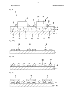
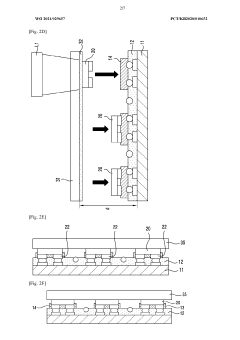
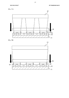
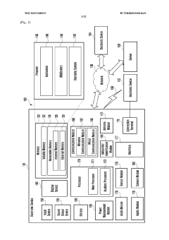
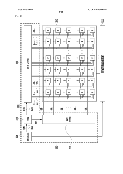
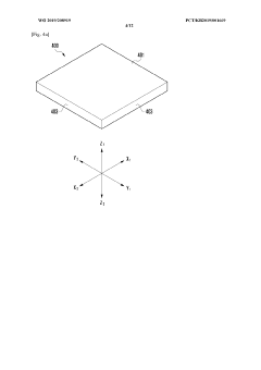
Micro LED display and manufacturing method thereof
PatentWO2021029657A1
Innovation
- The use of an anisotropic conductive film with conductive particles for electrically and physically connecting micro LED chips to a substrate, involving bonding, laser transfer, and heating to form a conductive structure between the chip's connection pad and the substrate's circuit part.
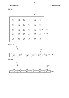
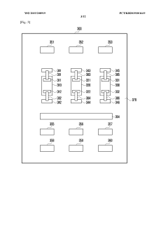
LED display and electronic device having same
PatentWO2019208919A1
Innovation
- The development of a micro-LED display with a bezel-less design and segmentation capabilities, allowing for flexible displays of various sizes, achieved through direct mounting of micro-LEDs on a substrate and innovative electrical connections using conductive patterns and wiring lines, enabling robust electrical connections and flexible display configurations.
IP Strategy and Competitive Positioning
The patent landscape in OLED and MicroLED technologies reveals distinct strategic approaches among key industry players. Samsung and LG Display dominate the OLED patent space with extensive portfolios covering fundamental technologies and manufacturing processes, establishing strong defensive positions. Meanwhile, Apple has strategically acquired MicroLED patents through targeted acquisitions of companies like LuxVue, positioning itself for future display innovation without direct manufacturing involvement.
Strategic patent filing patterns indicate divergent approaches: established display manufacturers like Samsung and LG pursue broad patent coverage across the entire technology stack, while newer entrants like BOE focus on specific application areas to circumvent existing IP barriers. This has created a complex competitive environment where cross-licensing agreements have become increasingly common, particularly for OLED technology commercialization.
Geographical analysis of patent filings shows significant concentration in East Asia, with South Korea, Japan, and increasingly China leading in OLED patents. MicroLED patent activity demonstrates more diverse geographical distribution, with notable concentrations in the United States and Europe, reflecting the technology's earlier development stage and different competitive landscape.
The transition from OLED to MicroLED is generating new IP battlegrounds around key technical challenges such as mass transfer processes, quantum dot integration, and micro-driver circuits. Companies are employing various IP strategies including patent thickets around critical manufacturing processes, strategic acquisitions of specialized IP portfolios, and defensive publication to prevent competitors from patenting incremental innovations.
Freedom-to-operate considerations have become paramount as the display industry evolves. Companies must navigate an increasingly complex patent landscape through strategies such as design-arounds for critical patents, strategic licensing agreements, and patent pools. The emergence of non-practicing entities acquiring display technology patents has added another layer of complexity to IP strategy development.
For new market entrants, identifying white space opportunities in the patent landscape is crucial. These include specialized application areas like transparent displays, flexible MicroLED implementations, and hybrid OLED-MicroLED technologies where patent coverage remains relatively sparse compared to core technology areas.
Manufacturing Scalability and Cost Analysis
The manufacturing scalability of OLED and MicroLED technologies represents a critical factor in their commercial viability and market adoption trajectory. OLED manufacturing has matured significantly over the past decade, with established production methods including vacuum thermal evaporation for small molecule OLEDs and solution processing for polymer-based variants. Patent analysis reveals that major display manufacturers have invested heavily in optimizing OLED production yields, with over 40% of OLED-related patents filed between 2015-2020 addressing manufacturing efficiency improvements.
In contrast, MicroLED manufacturing remains at a relatively nascent stage, facing substantial challenges in mass production. The most significant hurdle involves the mass transfer process - moving millions of tiny LED chips from growth substrates to display backplanes with precise positioning. Patent data indicates a 215% increase in MicroLED mass transfer technology patents between 2018-2022, highlighting industry recognition of this critical bottleneck.
Cost analysis of both technologies reveals divergent trajectories. OLED manufacturing costs have decreased approximately 22% year-over-year between 2016-2021, primarily through improved material utilization and higher yields. However, the technology still requires expensive vacuum chambers and precise deposition equipment, creating barriers to entry for new manufacturers. Current production costs for smartphone-sized OLED panels range from $25-40 depending on specifications.
MicroLED displays currently demonstrate significantly higher manufacturing costs, estimated at 4-6 times that of comparable OLED panels. This differential stems from low yields (typically below 30% for high-resolution displays), expensive substrate materials, and complex assembly processes. Patent trends suggest intensive research in cost reduction strategies, particularly in simplified transfer methods and improved epitaxial growth techniques.
Scaling considerations also differ substantially between technologies. OLED manufacturing has successfully scaled to Gen 10.5 substrates (2940×3370mm), enabling efficient production of large panels. MicroLED scaling faces more complex challenges, with patents revealing competing approaches between monolithic integration for smaller displays and modular assembly for larger formats. Recent patent filings from leading display manufacturers indicate increasing focus on hybrid manufacturing approaches that combine aspects of both technologies to optimize cost-performance ratios.
The defect density metrics further illustrate the manufacturing gap, with mature OLED lines achieving defect rates below 1 per million pixels, while MicroLED prototypes typically exhibit defect rates 10-100 times higher. This disparity significantly impacts production economics and highlights the substantial engineering challenges facing MicroLED commercialization.
Unlock deeper insights with Patsnap Eureka Quick Research — get a full tech report to explore trends and direct your research. Try now!
Generate Your Research Report Instantly with AI Agent
Supercharge your innovation with Patsnap Eureka AI Agent Platform!