OLED vs MicroLED: Achievements in Light Source Management
OCT 24, 20259 MIN READ
Generate Your Research Report Instantly with AI Agent
Patsnap Eureka helps you evaluate technical feasibility & market potential.
Display Technology Evolution and Objectives
Display technology has undergone remarkable evolution since the introduction of cathode ray tubes (CRTs) in the early 20th century. The progression from CRTs to liquid crystal displays (LCDs) marked the first major shift toward flatter, more energy-efficient screens. This transition set the foundation for subsequent innovations including plasma display panels (PDPs), which offered improved contrast ratios and viewing angles but suffered from high power consumption and screen burn-in issues.
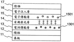
The introduction of Organic Light-Emitting Diode (OLED) technology in the late 1990s represented a paradigm shift in display technology. Unlike LCDs that require backlighting, OLED pixels emit light independently when electrical current passes through organic compounds. This self-emissive property enabled thinner displays, perfect blacks, wider viewing angles, and potentially lower power consumption, establishing OLED as the premium display technology for smartphones, televisions, and wearable devices.
Despite OLED's advantages, challenges including limited brightness, color shift at extreme viewing angles, and organic material degradation leading to burn-in have persisted. These limitations have driven research toward alternative technologies, with MicroLED emerging as the most promising successor. MicroLED technology utilizes microscopic inorganic LED arrays that offer superior brightness, longevity, and energy efficiency compared to OLED, while maintaining the self-emissive benefits.
The technical evolution in light source management between these technologies represents distinct approaches to achieving optimal visual performance. OLED technology has focused on refining organic materials and implementing sophisticated compensation algorithms to address inherent limitations. Innovations include advanced thin-film encapsulation techniques, pixel compensation circuits, and material refinements that have progressively improved lifetime and brightness capabilities.
MicroLED development has concentrated on overcoming manufacturing challenges related to mass transfer of microscopic LED elements and achieving consistent performance across millions of individual emitters. Recent breakthroughs in epitaxial growth processes and mass transfer techniques have accelerated MicroLED's path toward commercial viability, though cost remains a significant barrier to widespread adoption.
The primary objective in this technological evolution is to achieve the perfect display that combines the best attributes of both technologies: the perfect blacks and wide viewing angles of OLED with the brightness, longevity, and efficiency of MicroLED. Additional goals include reducing manufacturing costs, improving energy efficiency, enabling novel form factors such as transparent and flexible displays, and enhancing color accuracy across the visual spectrum.
Market Demand Analysis for Advanced Display Technologies
The display technology market is witnessing unprecedented growth driven by increasing consumer demand for superior visual experiences across multiple device categories. Current market analysis indicates that the global advanced display technology sector is expanding at a compound annual growth rate of approximately 8%, with particular acceleration in premium smartphone, television, and wearable device segments.
Consumer preferences are increasingly favoring displays with higher resolution, better color accuracy, improved energy efficiency, and thinner form factors. This shift is particularly evident in the high-end smartphone market, where manufacturers compete intensely on display quality as a key differentiating factor. The automotive industry represents another rapidly growing segment, with advanced displays becoming central to dashboard systems and entertainment consoles.
OLED technology currently dominates the premium display market due to its superior contrast ratios, flexible form factor capabilities, and excellent color reproduction. Market research shows that OLED displays command approximately 70% of the premium smartphone display market, with Samsung Display and LG Display as the primary manufacturers. However, OLED faces persistent challenges including burn-in issues, limited brightness in outdoor conditions, and relatively high production costs.
MicroLED technology, though still emerging, is generating significant market interest due to its potential advantages over OLED. Industry forecasts predict that the MicroLED market will grow substantially over the next five years as manufacturing processes mature and costs decrease. Early adopters are primarily in the luxury television and commercial display sectors, with Samsung, Sony, and Apple making significant investments in the technology.
Regional analysis reveals that East Asia continues to lead in both production capacity and consumption of advanced display technologies, with China rapidly expanding its manufacturing capabilities. North America and Europe represent significant markets primarily driven by consumer electronics and automotive applications.
The enterprise and commercial sectors are increasingly adopting large-format advanced displays for conference rooms, digital signage, and control centers. These applications demand higher brightness, longer lifespans, and better energy efficiency than consumer applications, creating a distinct market segment with specific technical requirements.
Market research indicates that consumers are willing to pay premium prices for devices with superior display quality, particularly when improvements in visual experience are immediately noticeable. This price elasticity has encouraged manufacturers to continue investing in advanced display technologies despite higher production costs, as they can command higher margins on premium products.
OLED and MicroLED Technical Challenges
Both OLED and MicroLED technologies face significant technical challenges that impact their performance, manufacturing processes, and market adoption. OLED technology, despite its commercial maturity, continues to struggle with several fundamental issues. Organic materials inherently degrade over time, particularly blue OLED emitters which have shorter lifespans compared to red and green counterparts. This differential aging leads to color shift and reduced brightness over the display's lifetime, requiring sophisticated compensation algorithms.
Power efficiency remains another critical challenge for OLED displays, especially when displaying bright content. The current density required for high brightness operation accelerates material degradation and increases power consumption, limiting their application in high-brightness environments like automotive displays or outdoor signage. Additionally, OLED displays suffer from burn-in effects when static images are displayed for extended periods, creating permanent ghost images.
Manufacturing scalability presents ongoing difficulties for OLED technology. The vacuum deposition processes used for OLED production are complex and expensive, with yield rates that decrease as panel sizes increase. This has limited OLED adoption in larger display formats and kept production costs relatively high despite years of optimization.
MicroLED technology, while promising superior performance characteristics, faces even more formidable manufacturing challenges. The mass transfer process—moving millions of tiny LED chips from growth substrates to display backplanes with perfect precision—remains the most significant hurdle. Current pick-and-place technologies struggle with throughput and placement accuracy at the microscale required for high-resolution displays.
Yield management is particularly problematic for MicroLED. A single defective LED in a display requires repair or replacement, and as display resolution increases, the sheer number of potential failure points grows exponentially. This challenge is compounded by the need for consistent performance across millions of individual LEDs in terms of brightness, color, and electrical characteristics.
Color conversion technology presents another obstacle for MicroLED displays. While blue LEDs are relatively efficient, creating red and green subpixels often requires phosphor or quantum dot conversion layers that can reduce efficiency and color purity. Developing direct-emission red and green MicroLEDs with comparable efficiency to blue remains an active research area.
Both technologies also face challenges in backplane technology integration. OLED requires precise current control for each pixel, while MicroLED needs high current density capabilities that push the limits of thin-film transistor technology, particularly for high-brightness applications. These technical hurdles directly impact manufacturing costs, device performance, and ultimately market adoption rates.
Current Light Source Management Solutions
01 Light emission efficiency optimization in OLED and MicroLED displays
Various techniques are employed to optimize light emission efficiency in OLED and MicroLED displays. These include specialized electrode designs, improved organic layer compositions, and advanced quantum dot implementations. By enhancing the quantum efficiency of emissive materials and optimizing the device structure, manufacturers can achieve higher brightness levels while reducing power consumption. These optimizations are crucial for extending battery life in portable devices and improving overall display performance.- Light emission control in OLED/MicroLED displays: Advanced control mechanisms for managing light emission in OLED and MicroLED displays. These technologies involve precise control of individual pixels or sub-pixels to optimize brightness, contrast, and power consumption. The systems typically include driving circuits that adjust current or voltage to each emitter based on display content and ambient conditions, resulting in improved visual performance and energy efficiency.
- Thermal management for display technologies: Thermal management solutions specifically designed for OLED and MicroLED displays to maintain optimal operating temperatures. These solutions address heat dissipation challenges through innovative materials, structures, and cooling mechanisms. Effective thermal management prevents performance degradation, extends device lifespan, and ensures consistent light output across the display surface, particularly important for high-brightness applications.
- Optical enhancement techniques: Methods and structures for enhancing the optical properties of OLED and MicroLED displays. These include specialized films, lenses, diffusers, and reflectors that improve light extraction efficiency, viewing angles, and color accuracy. By optimizing the path of emitted light, these techniques increase brightness while reducing power consumption, and can help mitigate issues like ambient light reflection and color shift at wide viewing angles.
- Pixel architecture and arrangement: Innovative pixel architectures and arrangements for OLED and MicroLED displays that optimize light output and efficiency. These designs include sub-pixel configurations, pixel density optimization, and novel emitter layouts that enhance resolution, color reproduction, and power efficiency. Advanced pixel architectures can also incorporate features for improved reliability, reduced crosstalk between pixels, and better integration with driving circuitry.
- Adaptive brightness and power management: Systems for dynamically adjusting display brightness and power consumption based on content, ambient conditions, and user preferences. These technologies incorporate sensors and algorithms to optimize light output for different viewing environments while preserving battery life. Adaptive management can selectively dim or brighten specific screen areas, adjust refresh rates, or modify color profiles to maintain visual quality while minimizing energy usage.
02 Thermal management systems for display technologies
Thermal management is critical in OLED and MicroLED displays to maintain optimal performance and longevity. Advanced heat dissipation structures, including specialized substrates and heat sinks, help regulate operating temperatures. Some designs incorporate phase-change materials or active cooling systems to manage heat during high-brightness operation. Effective thermal management prevents degradation of organic materials in OLEDs and maintains consistent light output in MicroLEDs, ultimately extending the lifespan of the display.Expand Specific Solutions03 Color management and gamut enhancement techniques
Color management systems in OLED and MicroLED displays utilize advanced algorithms and hardware solutions to achieve wider color gamuts and more accurate color reproduction. These techniques include color filters, quantum dot enhancement films, and specialized pixel architectures. By precisely controlling the spectral output of individual light-emitting elements, these technologies can produce more vibrant and accurate colors. Some implementations also incorporate ambient light sensing to dynamically adjust color profiles based on viewing conditions.Expand Specific Solutions04 Power efficiency and brightness control mechanisms
Advanced power management systems in OLED and MicroLED displays enable dynamic control of brightness levels while optimizing energy consumption. These mechanisms include pixel-level dimming, regional backlight control, and adaptive refresh rates. By selectively controlling the power delivered to different display regions based on content, these technologies can significantly reduce energy consumption while maintaining visual quality. Some implementations also incorporate ambient light sensors to automatically adjust brightness levels according to environmental conditions.Expand Specific Solutions05 Pixel architecture and light distribution optimization
Innovative pixel architectures in OLED and MicroLED displays focus on optimizing light distribution and reducing optical losses. These designs include specialized micro-lenses, light-guiding structures, and reflective elements that help direct emitted light toward the viewer. By minimizing internal reflection and light trapping, these technologies improve the overall efficiency of the display. Some implementations also incorporate sub-pixel arrangements that enhance resolution while maintaining color accuracy and viewing angles.Expand Specific Solutions
Key Industry Players in Display Manufacturing
The OLED vs MicroLED display technology landscape is currently in a transitional phase, with OLED being mature and commercially widespread while MicroLED remains in early commercialization. The global market for these advanced display technologies is projected to exceed $200 billion by 2025, driven by demand for higher performance displays. In terms of technical maturity, Samsung Display, BOE Technology, and Universal Display Corporation lead OLED development with established manufacturing capabilities, while companies like Samsung Electronics, Rohinni, and Lumileds are pioneering MicroLED advancements. Apple's acquisition of LuxVue and subsequent patents indicate growing interest in MicroLED as the potential successor to OLED, particularly for applications requiring higher brightness, efficiency, and longevity.
BOE Technology Group Co., Ltd.
Technical Solution: BOE Technology has developed comprehensive solutions for both OLED and MicroLED display technologies with significant innovations in light source management. For OLED, BOE has implemented advanced Oxide TFT backplane technology that enables more precise current delivery to each pixel, resulting in more uniform brightness and extended panel lifetime. Their OLED manufacturing process incorporates specialized color filter technology that enhances color gamut coverage to over 110% DCI-P3 while improving light extraction efficiency. BOE's OLED panels feature multi-layer thin film encapsulation with moisture-resistant barriers that extend operational lifetime while maintaining flexibility. In the MicroLED space, BOE has developed a proprietary "active matrix" driving architecture that enables individual pixel control with minimal crosstalk. Their MicroLED implementation utilizes chip-on-board technology with specialized phosphor conversion layers to achieve full-color displays from monochromatic LED chips, significantly simplifying the manufacturing process. BOE has also pioneered hybrid transfer techniques that combine mechanical and laser-assisted processes to place microLEDs with high precision and yield.
Strengths: Massive production capacity with multiple advanced display manufacturing facilities; vertical integration from backplane to module assembly; strong R&D capabilities with thousands of display patents. Weaknesses: Still catching up to Samsung and LG in high-end OLED manufacturing yield rates; MicroLED technology remains primarily in development phase rather than mass production; higher defect rates in initial production runs compared to more established competitors.
Samsung Electronics Co., Ltd.
Technical Solution: Samsung Electronics has pioneered significant advancements in both OLED and MicroLED technologies. For OLED, Samsung has developed Quantum Dot OLED (QD-OLED) technology that combines quantum dots with OLED to achieve superior color volume and brightness efficiency. Their OLED panels utilize a blue OLED emitter layer with quantum dot color conversion layers to produce red and green light, resulting in improved color purity and wider color gamut compared to traditional OLED displays. In MicroLED development, Samsung has introduced "The Wall" - a modular MicroLED display system using inorganic LED technology with micrometer-sized LEDs that act as individual pixels. Samsung's MicroLED implementation achieves brightness levels exceeding 2,000 nits while maintaining perfect black levels through individual pixel control. Their light source management includes proprietary surface treatments to minimize reflection and enhance contrast in various lighting conditions.
Strengths: Industry-leading production capacity for both technologies; proprietary quantum dot enhancement for OLED; modular design approach for MicroLED allowing scalable display sizes. Weaknesses: High manufacturing costs for MicroLED due to complex transfer and placement processes; OLED technology still faces burn-in concerns with static content despite mitigation efforts.
Breakthrough Patents in Emission Efficiency
Organic light-emitting diode apparatus
PatentActiveUS20160148560A1
Innovation
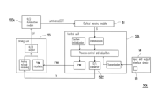
- An OLED apparatus comprising an OLED illumination module, a driving unit, an optical sensing module, and a control unit that adjusts voltage and duty cycle of pulse width modulation (PWM) to dynamically change CCT and light intensity, utilizing a storage unit to store photoelectric parameter data for target adjustments.
Organic light-emitting diode and method of fabricating the same
PatentInactiveTW201125431A
Innovation
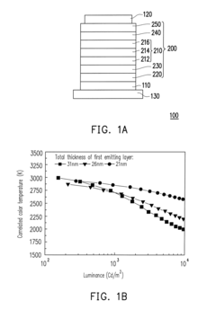
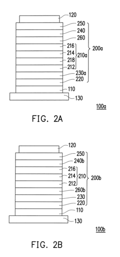
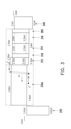
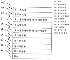
- The OLED device structure includes multiple light-emitting layers with specific compositions near the anode and cathode ends, allowing it to emit different wavelengths of visible light based on voltage, enabling white light or other colors with specific color temperatures through voltage adjustment alone.
Energy Efficiency Comparison and Environmental Impact
The energy efficiency comparison between OLED and MicroLED technologies reveals significant differences in power consumption patterns and environmental implications. OLED displays demonstrate superior efficiency in displaying darker content due to their emissive nature, where black pixels consume virtually no power. This characteristic makes OLEDs particularly energy-efficient for applications with predominantly dark interfaces or content, such as mobile devices with dark mode.
MicroLED technology, while still evolving, shows promising efficiency metrics in high-brightness scenarios. Current data indicates that MicroLEDs can achieve up to 30% greater energy efficiency than OLEDs when displaying bright, full-screen content. This advantage stems from MicroLED's higher luminous efficacy, measured at approximately 30-50 lumens per watt compared to OLED's 20-40 lumens per watt in commercial applications.
The environmental impact assessment of both technologies extends beyond operational energy consumption to manufacturing processes and end-of-life considerations. OLED production currently involves organic solvents and rare materials that present environmental challenges, including potential groundwater contamination if improperly handled. The manufacturing carbon footprint of OLED displays remains substantial, with estimates suggesting 85-110 kg CO2 equivalent per square meter of display area.
MicroLED manufacturing, while less mature at scale, presents its own environmental considerations. The production process requires fewer toxic organic compounds but demands precise fabrication techniques that are energy-intensive. Early lifecycle assessments suggest MicroLED manufacturing may eventually achieve a 15-25% reduction in carbon footprint compared to OLED, though current limited-scale production does not yet realize these benefits.
Longevity factors significantly into the environmental equation. MicroLED's theoretical lifespan of 100,000+ hours substantially exceeds OLED's typical 30,000-60,000 hours before significant brightness degradation occurs. This extended operational life potentially reduces electronic waste generation by decreasing replacement frequency, though this advantage remains largely theoretical until widespread commercial deployment provides real-world validation.
Water usage presents another environmental consideration, with OLED manufacturing requiring approximately 30-45 liters per square meter of display, while preliminary MicroLED production data suggests comparable or slightly lower requirements. However, the specialized cleaning processes in MicroLED manufacturing may introduce different water purification challenges that require further assessment as production scales.
Supply Chain Analysis and Manufacturing Scalability
The OLED and MicroLED supply chains present distinct challenges and opportunities that significantly impact their market adoption and technological advancement. OLED manufacturing has matured considerably over the past decade, with established supply chains primarily dominated by South Korean giants like Samsung and LG Display, alongside emerging Chinese manufacturers. The OLED ecosystem benefits from years of investment in production infrastructure, with relatively stabilized material sourcing networks for organic compounds, though certain rare materials remain subject to supply constraints.
In contrast, MicroLED supply chains are still in nascent stages of development, characterized by fragmentation and technological uncertainty. The manufacturing process requires unprecedented precision in mass transfer techniques to place millions of microscopic LED chips accurately. This complexity has resulted in specialized segments within the supply chain, with different companies focusing on specific components: LED epitaxy growth, chip manufacturing, mass transfer equipment, and integration technologies.
Production scalability represents perhaps the most significant differentiator between these technologies. OLED manufacturing has achieved economies of scale through generations of fabrication facilities, with Gen 10.5 fabs now operational for large panels. Yield rates have improved substantially, though they still present challenges for complex implementations like foldable displays. The established vapor deposition processes allow for relatively efficient scaling of production volumes.
MicroLED faces formidable scalability hurdles, primarily centered around the mass transfer process and microscopic repair techniques. Current manufacturing approaches remain largely experimental or limited to small-batch production for premium applications. The requirement for near-perfect yield in LED chip placement (99.9999%) presents unprecedented manufacturing challenges, as a single defective pixel is visually apparent in the final display.
Cost structures reflect these supply chain realities. OLED production costs have decreased steadily but plateaued in recent years due to fundamental material and process limitations. MicroLED costs remain prohibitively high for mass-market applications, with estimates suggesting they are currently 5-10 times more expensive than equivalent OLED displays, primarily due to complex manufacturing processes and low yields.
Regional manufacturing capabilities also shape the competitive landscape, with East Asian countries dominating OLED production, while MicroLED development shows a more globally distributed pattern, with significant research activities in North America and Europe alongside Asian manufacturing expertise.
Unlock deeper insights with Patsnap Eureka Quick Research — get a full tech report to explore trends and direct your research. Try now!
Generate Your Research Report Instantly with AI Agent
Supercharge your innovation with Patsnap Eureka AI Agent Platform!
