

OLED vs MicroLED: Evaluating Regulatory Frameworks
OCT 24, 202510 MIN READ
Generate Your Research Report Instantly with AI Agent
Patsnap Eureka helps you evaluate technical feasibility & market potential.
OLED and MicroLED Technology Evolution and Objectives
The evolution of display technologies has witnessed significant advancements over the past decades, with OLED (Organic Light-Emitting Diode) and MicroLED emerging as cutting-edge solutions that promise to revolutionize visual experiences across multiple industries. OLED technology, first conceptualized in the 1950s, saw practical development in the 1980s by Eastman Kodak, with commercial applications beginning in the early 2000s. The technology has since evolved from passive-matrix to active-matrix configurations, enabling higher resolution and improved energy efficiency.
MicroLED represents a more recent technological innovation, with foundational research beginning in the early 2000s. Unlike OLED, which utilizes organic compounds, MicroLED employs inorganic gallium nitride-based materials to create self-emissive pixels at microscopic scales. This fundamental difference has significant implications for performance characteristics, manufacturing processes, and regulatory considerations.
The technological trajectory for both display technologies has been driven by several key objectives: achieving higher energy efficiency, extending operational lifespan, enhancing brightness and color accuracy, reducing production costs, and minimizing environmental impact. These objectives align with broader industry trends toward sustainable and high-performance consumer electronics.
Current OLED technology has reached maturity in several applications, particularly in smartphones and high-end televisions, while continuing to evolve in flexible and transparent display implementations. The technology offers exceptional contrast ratios and color reproduction but faces challenges related to brightness limitations, blue pixel degradation, and manufacturing scalability.
MicroLED technology, while still in earlier stages of commercial deployment, demonstrates promising advantages in brightness capability, energy efficiency, and theoretical lifespan. However, it currently faces significant manufacturing challenges, particularly in mass transfer processes and yield rates for large-scale production.
The regulatory landscape surrounding these technologies has evolved alongside their technical development. Early frameworks primarily addressed basic safety concerns, while contemporary regulations increasingly focus on energy efficiency standards, hazardous material restrictions, end-of-life management, and sustainability metrics. This evolution reflects growing awareness of environmental impacts and resource constraints.
Looking forward, both technologies are expected to continue advancing along parallel but distinct paths. OLED development is likely to focus on addressing longevity concerns, enhancing brightness capabilities, and reducing production costs through improved manufacturing processes. MicroLED research will prioritize solving mass production challenges, reducing pixel size, and developing more efficient assembly techniques to enable broader commercial adoption.
Market Demand Analysis for Advanced Display Technologies
The display technology market is witnessing unprecedented growth driven by increasing consumer demand for superior visual experiences across multiple devices. Current market analysis indicates that the global advanced display market is projected to reach $167 billion by 2025, with OLED technology currently dominating premium segments while MicroLED emerges as a promising contender. This growth trajectory is supported by expanding applications in smartphones, televisions, wearables, automotive displays, and commercial signage.
Consumer preferences are increasingly favoring thinner, more energy-efficient displays with higher resolution, better color accuracy, and longer lifespans. OLED technology has established strong market penetration due to its superior contrast ratios, flexibility, and energy efficiency in small to medium-sized applications. Market research shows that OLED displays currently command approximately 30% of the premium smartphone market and are rapidly expanding in the television sector with annual growth rates exceeding 15%.
MicroLED technology, though still in early commercialization phases, is generating significant market interest due to its potential advantages in brightness, longevity, and energy efficiency. Industry forecasts suggest MicroLED could capture 10% of the high-end display market by 2027, particularly in premium television and commercial display segments where its superior brightness and durability justify higher price points.
Regional analysis reveals differentiated market demands, with North American and European consumers prioritizing image quality and energy efficiency, while Asian markets show stronger preference for innovative form factors and competitive pricing. This regional variation significantly impacts regulatory approaches and market entry strategies for both technologies.
The automotive sector represents one of the fastest-growing segments for advanced display technologies, with projected compound annual growth rates of 18% through 2026. Both OLED and MicroLED are competing for dominance in this space, with regulatory requirements for durability and reliability playing a crucial role in technology adoption.
Enterprise and commercial applications present another substantial market opportunity, with digital signage and control room displays increasingly adopting advanced display technologies. This segment values longevity and reliability, areas where MicroLED potentially offers advantages over OLED, though regulatory certification processes for these applications remain complex and varied across regions.
Consumer electronics manufacturers are increasingly factoring regulatory compliance costs into their technology roadmaps, with some estimates suggesting that regulatory certification and compliance can represent up to 8% of total development costs for new display products. This economic reality is shaping investment decisions between OLED and MicroLED technologies, particularly for global product launches requiring multiple regulatory approvals.
Current Technical Challenges and Regulatory Constraints
Both OLED and MicroLED technologies face significant technical challenges and regulatory constraints that impact their development and market adoption. OLED technology, despite its commercial maturity, continues to struggle with issues related to blue pixel degradation, resulting in shorter lifespans compared to other color pixels. This differential aging creates color balance problems over time, particularly affecting display longevity in high-end consumer electronics. Additionally, OLED manufacturing processes involve organic materials that require stringent environmental controls during production.
MicroLED, while promising superior performance, faces even greater technical hurdles. The mass transfer process—moving millions of microscopic LED chips precisely onto display substrates—remains a significant manufacturing challenge. Current yield rates are suboptimal, driving up production costs and limiting commercial viability. The miniaturization of LED chips below 10 micrometers introduces quantum effects that can alter emission properties, requiring further research to maintain consistent performance.
From a regulatory perspective, both technologies must navigate complex frameworks across different jurisdictions. OLED manufacturing involves potentially hazardous organic compounds and solvents that fall under strict chemical safety regulations, including REACH in Europe and similar frameworks in North America and Asia. Manufacturers must comply with extensive documentation requirements and substance restrictions that vary by region, creating compliance complexity for global operations.
MicroLED faces emerging regulatory questions regarding the use of rare earth elements in LED phosphors, with increasing scrutiny on sustainable sourcing and potential supply chain regulations. Additionally, both technologies must address end-of-life considerations, with the EU's WEEE Directive and similar regulations worldwide requiring manufacturers to establish recycling programs and minimize electronic waste.
Energy efficiency standards present another regulatory dimension, with different regions implementing varying requirements for display power consumption. While both technologies offer energy advantages over traditional LCD displays, they must still meet increasingly stringent energy efficiency certifications to access certain markets, particularly in the EU and California.
Intellectual property protection represents a significant constraint for both technologies, with complex patent landscapes creating potential barriers to innovation. OLED technology features numerous overlapping patents controlled by major manufacturers, while MicroLED's emerging status has triggered aggressive patent filing activity, potentially leading to future litigation as the technology commercializes.
Radiation safety regulations also apply to both technologies, requiring compliance with electromagnetic emission standards and blue light exposure limits, with regulatory bodies increasingly concerned about potential health impacts of display technologies on users, particularly children.
Comparative Analysis of OLED and MicroLED Solutions
01 Regulatory compliance for OLED and MicroLED displays
Display technologies such as OLED and MicroLED must comply with various regulatory frameworks that govern electronic devices. These regulations typically address safety standards, electromagnetic compatibility, energy efficiency requirements, and environmental considerations. Manufacturers must ensure their display technologies meet these regulatory requirements before market introduction, which may include certification processes and compliance testing for different regions.- Safety and emission standards for OLED and MicroLED displays: Regulatory frameworks for OLED and MicroLED displays include safety standards related to electromagnetic emissions, blue light exposure limits, and hazardous material restrictions. These regulations ensure that display technologies comply with health and safety requirements across different jurisdictions, particularly regarding eye safety and radiation exposure. Manufacturers must design their displays to meet these standards while maintaining performance characteristics.
- Environmental compliance and sustainability regulations: OLED and MicroLED display technologies are subject to environmental regulations governing manufacturing processes, material usage, and end-of-life disposal. These include restrictions on hazardous substances, energy efficiency requirements, and recycling mandates. Manufacturers must demonstrate compliance with frameworks like RoHS, WEEE, and energy star ratings, while developing more sustainable production methods and materials to reduce environmental impact.
- Certification and testing protocols for display technologies: Regulatory frameworks establish specific certification and testing protocols that OLED and MicroLED displays must undergo before market approval. These include performance testing for brightness, contrast, color accuracy, and durability. Standardized testing methodologies ensure consistency across manufacturers and provide consumers with reliable information about display quality and performance characteristics. Certification marks indicate compliance with relevant standards and regulations.
- Intellectual property and patent regulations: The regulatory landscape for OLED and MicroLED technologies includes intellectual property frameworks governing patents, trademarks, and trade secrets. These regulations impact how companies can develop, license, and commercialize display innovations. Patent pools, cross-licensing agreements, and standard-essential patents play important roles in the industry's development. Companies must navigate complex IP regulations across different jurisdictions while protecting their innovations and avoiding infringement.
- Market access and import/export regulations: OLED and MicroLED display manufacturers must comply with market access regulations including import/export controls, tariffs, and regional technical standards. These regulations vary by country and region, creating a complex compliance landscape for global distribution. Companies must obtain necessary certifications and approvals for each market, while navigating trade restrictions, customs requirements, and localization standards that may impact product specifications and marketing claims.
02 Environmental and sustainability regulations for display technologies
OLED and MicroLED display technologies are subject to environmental regulations that address material usage, energy consumption, and end-of-life disposal. These frameworks often include restrictions on hazardous substances, requirements for recyclability, and energy efficiency standards. Manufacturers must design their display technologies to comply with regulations such as RoHS (Restriction of Hazardous Substances), WEEE (Waste Electrical and Electronic Equipment), and various energy efficiency directives.Expand Specific Solutions03 Safety standards and certification requirements
OLED and MicroLED displays must meet specific safety standards and certification requirements before they can be marketed. These include electrical safety standards, flicker regulations, blue light emission limits, and other health and safety considerations. Display manufacturers need to obtain certifications from relevant regulatory bodies and ensure their products meet the safety requirements for consumer electronics in different markets.Expand Specific Solutions04 Intellectual property regulations and patent frameworks
The development and commercialization of OLED and MicroLED technologies are heavily influenced by intellectual property regulations. Patent frameworks govern how innovations in display technologies can be protected, licensed, and enforced. Companies must navigate complex patent landscapes to avoid infringement while protecting their own innovations in areas such as pixel structures, manufacturing processes, and materials used in these advanced display technologies.Expand Specific Solutions05 Market-specific regulatory requirements for display technologies
OLED and MicroLED display manufacturers must comply with region-specific regulatory frameworks that vary across different markets. These include unique certification requirements, labeling standards, and technical specifications that may differ between North America, Europe, Asia, and other regions. Companies developing display technologies need to adapt their products to meet these varying requirements, which may include different testing protocols and documentation for each market they enter.Expand Specific Solutions
Key Industry Players and Competitive Landscape
The OLED vs MicroLED regulatory landscape reflects an industry in transition, with OLED technology in mature commercialization while MicroLED remains in early development stages. The global display market, valued at approximately $150 billion, shows increasing regulatory focus on energy efficiency standards and hazardous materials restrictions. BOE Technology Group, Samsung Electronics, and LG Display lead OLED commercialization with established compliance frameworks, while companies like Applied Materials and Universal Display Corporation navigate emerging MicroLED regulations. Smaller players like Lumileds and eMagin face challenges adapting to evolving standards across different jurisdictions, particularly regarding environmental impact and end-of-life disposal requirements.
BOE Technology Group Co., Ltd.
Technical Solution: BOE has developed an integrated regulatory compliance platform called "DisplayRegTech" that addresses both OLED and MicroLED technologies. Their approach focuses on harmonizing compliance across different jurisdictions while accounting for the distinct regulatory challenges of each display technology. For OLED, BOE's system emphasizes chemical safety regulations compliance, particularly for the handling and disposal of organic materials used in manufacturing. Their MicroLED regulatory framework concentrates on emerging standards for energy efficiency, as MicroLED promises significant power consumption advantages that may require new testing methodologies to properly evaluate. BOE actively engages with Chinese regulatory authorities to help develop national standards that can influence international frameworks, particularly in energy efficiency metrics and hazardous substance limitations. The company maintains a regulatory database that tracks over 120 display-specific regulations across 35 countries, with automated compliance verification tools that help product teams ensure designs meet all applicable requirements before manufacturing begins.
Strengths: Strong influence on Chinese regulatory standards which increasingly impact global markets; Integrated compliance systems covering both technologies; Sophisticated regulatory tracking tools. Weaknesses: International regulatory influence outside Asia still developing; Compliance resources sometimes constrained by rapid business expansion; Regulatory strategy sometimes reactive rather than proactive in Western markets.
Samsung Electronics Co., Ltd.
Technical Solution: Samsung has developed a comprehensive regulatory compliance framework for both OLED and MicroLED technologies. Their approach includes a dedicated Environmental Compliance Management System that addresses the specific challenges of each display technology. For OLED, Samsung focuses on managing organic materials disposal and recycling programs that comply with EU's WEEE and RoHS directives. Their MicroLED regulatory strategy emphasizes radiation safety standards compliance and electromagnetic compatibility testing protocols. Samsung actively participates in international standards development through organizations like IEC and ISO, helping shape future regulatory frameworks for next-generation display technologies. The company maintains specialized regulatory affairs teams in major markets to ensure regional compliance variations are addressed proactively rather than reactively, particularly focusing on emerging regulations around energy efficiency standards and end-of-life management for both technologies.
Strengths: Global regulatory expertise with established relationships with regulatory bodies worldwide; Comprehensive internal compliance systems tailored to different display technologies; Proactive approach to emerging regulations. Weaknesses: Complex global supply chain creates compliance challenges; Higher compliance costs compared to smaller competitors; Regulatory strategies sometimes prioritize established markets over emerging ones.
Patent Landscape and Intellectual Property Considerations
Anisotropic conductive film and display device
PatentActiveUS20220102326A1
Innovation
- An anisotropic conductive film with a first region of discretely arranged conductive particles corresponding to electrode patterns and a second region with aggregated conductive particles acting as an alignment marker, facilitating easy alignment with the circuit substrate and reducing production costs by forming alignment markers through conductive particle dispersion.
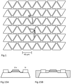
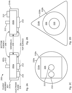
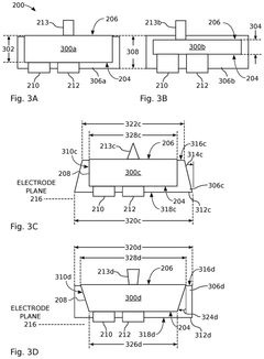
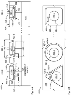
Encapsulated light emitting diodes for selective fluidic assembly
PatentActiveUS12119432B2
Innovation
- The use of partially encapsulated semiconductor-based inorganic micro-LEDs with a patternable polymer encapsulant that protects the LEDs from collisions and optimizes their shape for efficient assembly, allowing for higher speed and yield while preventing defects, and enabling precise alignment of LED colors on a display substrate.
Global Regulatory Frameworks and Compliance Requirements
The regulatory landscape for display technologies like OLED and MicroLED varies significantly across global markets, creating a complex compliance environment for manufacturers and distributors. In the United States, the Federal Communications Commission (FCC) regulates electronic displays through electromagnetic compatibility requirements, while the Environmental Protection Agency (EPA) enforces standards related to energy efficiency through programs like ENERGY STAR. Additionally, California's specific regulations on hazardous substances often exceed federal requirements, creating a higher compliance threshold for the entire US market.
The European Union implements more stringent regulatory frameworks through directives such as the Restriction of Hazardous Substances (RoHS), which limits the use of certain hazardous materials in electronic equipment, and the Waste Electrical and Electronic Equipment (WEEE) directive, which establishes collection, recycling, and recovery targets. The EU's Registration, Evaluation, Authorization and Restriction of Chemicals (REACH) regulation further impacts display manufacturers by requiring detailed reporting on chemical substances used in production.
In Asia, regulatory approaches differ substantially between countries. Japan's High Efficiency Electrical Appliance Certification system imposes strict energy efficiency standards, while China's Compulsory Certification System (CCC) requires rigorous safety testing and certification before market entry. South Korea, a major producer of display technologies, implements the Korean RoHS and energy efficiency standards that closely align with international frameworks but include country-specific requirements.
Emerging markets present additional regulatory challenges, with countries like India developing their own frameworks through initiatives such as the Electronic Waste Management Rules and Bureau of Indian Standards (BIS) certification requirements. These developing regulatory systems often incorporate elements from established frameworks while addressing local environmental and economic priorities.
For both OLED and MicroLED technologies, compliance with these diverse regulatory requirements necessitates significant investment in testing, certification, and documentation. MicroLED manufacturers face particular challenges related to novel materials and manufacturing processes that may not fit neatly into existing regulatory categories, potentially requiring additional safety assessments and environmental impact studies.
Industry standards organizations such as the International Electrotechnical Commission (IEC) and the International Organization for Standardization (ISO) play crucial roles in harmonizing technical requirements across jurisdictions, though significant regional variations persist. Manufacturers increasingly adopt comprehensive compliance management systems to navigate this complex global regulatory landscape, often exceeding minimum requirements to ensure access to all major markets.
Environmental Impact and Sustainability Considerations
The environmental impact of display technologies has become a critical consideration in regulatory frameworks governing OLED and MicroLED technologies. Both technologies present distinct environmental profiles throughout their lifecycle, from raw material extraction to end-of-life disposal, which regulators must carefully evaluate when developing sustainability standards.
OLED displays utilize organic compounds that require fewer rare earth elements compared to traditional LCD technologies, potentially reducing environmental damage from mining operations. However, the manufacturing process involves hazardous chemicals and solvents that pose environmental risks if not properly managed. Current regulations in the EU, particularly under the Restriction of Hazardous Substances (RoHS) directive, impose strict limitations on these substances, requiring manufacturers to develop alternative production methods.
MicroLED technology, while promising significant energy efficiency improvements, presents its own environmental challenges. The production process requires ultra-precise manufacturing techniques that consume substantial energy and water resources. Additionally, the gallium nitride semiconductors used in MicroLED production involve complex extraction processes with potential environmental consequences that are still being studied by regulatory bodies.
Energy consumption during operation represents a key sustainability metric under regulatory scrutiny. MicroLED displays demonstrate superior energy efficiency compared to OLEDs, particularly when displaying bright content, potentially reducing carbon footprints over product lifespans. This advantage has prompted several jurisdictions to consider energy efficiency incentives specifically targeting MicroLED adoption in public infrastructure and commercial applications.
End-of-life considerations present significant regulatory challenges for both technologies. OLED panels contain organic materials that may leach into soil and groundwater if improperly disposed of, while MicroLED displays contain minute semiconductor components that complicate recycling efforts. The EU's Waste Electrical and Electronic Equipment (WEEE) directive currently addresses some aspects of display disposal, but regulatory frameworks specifically tailored to these newer technologies remain underdeveloped.
Carbon footprint assessments across complete product lifecycles are increasingly being incorporated into regulatory frameworks. Recent lifecycle analyses indicate that while MicroLED manufacturing currently generates higher initial carbon emissions, the extended operational lifespan and superior energy efficiency may result in lower overall environmental impact. Regulators in several Asian manufacturing hubs have begun implementing carbon taxation schemes that directly impact production decisions for both technologies.
Water usage represents another critical environmental consideration, with MicroLED fabrication facilities typically requiring significant quantities of ultra-pure water. Emerging regulations in water-stressed regions are beginning to impose stricter limitations on industrial water consumption, potentially affecting manufacturing location decisions and production costs for display manufacturers.
Unlock deeper insights with Patsnap Eureka Quick Research — get a full tech report to explore trends and direct your research. Try now!
Generate Your Research Report Instantly with AI Agent
Supercharge your innovation with Patsnap Eureka AI Agent Platform!