

How OLED vs MicroLED Parameters Affect Visual Quality
OCT 24, 20259 MIN READ
Generate Your Research Report Instantly with AI Agent
Patsnap Eureka helps you evaluate technical feasibility & market potential.
OLED and MicroLED Display Technology Evolution
Display technology has undergone significant evolution since the introduction of cathode ray tubes (CRTs) in the early 20th century. The transition from CRTs to liquid crystal displays (LCDs) marked the first major shift toward flat panel technologies, enabling thinner devices with improved energy efficiency. The subsequent development of OLED (Organic Light Emitting Diode) technology in the late 1990s represented another revolutionary step, offering superior contrast ratios, wider viewing angles, and the ability to create flexible displays.
OLED technology operates on the principle of electroluminescence, where organic compounds emit light when an electric current passes through them. This self-emissive characteristic eliminates the need for backlighting, allowing for true blacks and infinite contrast ratios. The commercialization of OLED displays began in the early 2000s, initially in small devices like mobile phones and digital cameras, before expanding to larger applications such as televisions and monitors.
MicroLED technology emerged as a promising next-generation display technology around 2010. Unlike OLEDs, MicroLEDs utilize inorganic gallium nitride (GaN) materials to create microscopic LED arrays that function as individual pixels. Each MicroLED element is typically less than 100 micrometers in size, enabling extremely high-resolution displays with unprecedented brightness capabilities.
The technical evolution of both technologies has followed distinct trajectories. OLED development has focused on overcoming inherent limitations such as burn-in issues, limited lifespan of organic materials (particularly blue OLEDs), and manufacturing yield challenges for larger panels. Innovations like WOLED (White OLED) with color filters and TOLED (Transparent OLED) have expanded application possibilities.
MicroLED development has concentrated on miniaturization processes, mass transfer techniques for placing millions of tiny LEDs precisely, and reducing production costs. The technology has progressed from early prototypes with pixel sizes of hundreds of micrometers to current versions approaching 10 micrometers, enabling higher pixel densities suitable for consumer applications.
Recent technological advancements have seen the emergence of hybrid approaches, such as QD-OLED (Quantum Dot OLED) displays that combine quantum dot color conversion technology with OLED light emission to achieve wider color gamuts and improved efficiency. Similarly, Mini-LED backlighting has emerged as an intermediate technology, enhancing LCD performance while the industry works toward mainstream MicroLED adoption.
The evolution continues with research into more efficient materials, improved manufacturing processes, and novel form factors. Foldable and rollable OLED displays have already reached commercial markets, while transparent and stretchable variants are in advanced development stages. For MicroLED, the focus remains on scaling down production costs while maintaining the technology's inherent advantages in brightness, longevity, and energy efficiency.
Market Demand Analysis for Premium Display Technologies
The premium display technology market is experiencing unprecedented growth, driven by consumer demand for superior visual experiences across multiple device categories. Current market analysis indicates that high-end smartphones, televisions, and professional monitors represent the primary segments fueling this expansion, with emerging applications in automotive displays, virtual/augmented reality headsets, and digital signage creating additional momentum.
Consumer expectations have evolved dramatically in recent years, with end-users increasingly prioritizing display quality as a decisive purchasing factor. Market surveys reveal that consumers are willing to pay premium prices for devices featuring superior color accuracy, contrast ratios, brightness levels, and energy efficiency. This trend is particularly pronounced in the smartphone sector, where display quality has become a key differentiator among flagship devices.
The professional market segment demonstrates even stronger demand patterns, with content creators, designers, and medical imaging specialists requiring displays that offer exceptional color reproduction, resolution, and reliability. These professional users represent a smaller but highly profitable market segment willing to invest substantially in cutting-edge display technologies that enhance workflow efficiency and output quality.
Regional analysis shows Asia-Pacific leading global demand, with China, South Korea, and Japan serving as both major manufacturing hubs and consumption markets. North America and Europe follow closely, driven by high disposable incomes and rapid technology adoption rates. Emerging markets in India and Southeast Asia are showing accelerated growth trajectories as smartphone penetration increases and consumer electronics become more accessible.
Industry forecasts project the premium display technology market to maintain a compound annual growth rate exceeding 15% through 2028, with OLED currently dominating but MicroLED gaining significant traction. This growth is supported by expanding applications across multiple industries and increasing consumer willingness to upgrade devices specifically for display improvements.
The sustainability factor is emerging as an increasingly important market driver, with energy-efficient display technologies gaining favor among environmentally conscious consumers and businesses seeking to reduce operational costs. This trend particularly benefits MicroLED technology, which offers superior energy efficiency compared to traditional display technologies.
Market research indicates that visual quality parameters most valued by consumers include contrast ratio, color accuracy, brightness, viewing angles, and motion handling capabilities. As OLED and MicroLED technologies continue to evolve, manufacturers that can optimize these parameters while addressing cost concerns will likely capture larger market shares in this highly competitive landscape.
Current Technical Limitations and Challenges
Despite significant advancements in display technologies, both OLED and MicroLED face distinct technical limitations that impact their visual quality performance. OLED technology continues to struggle with brightness limitations, typically achieving 500-1000 nits in consumer devices, which restricts HDR performance and outdoor visibility. This ceiling exists because increasing brightness accelerates organic material degradation, creating a fundamental trade-off between luminance and panel lifespan.
Differential aging remains a critical challenge for OLED displays, where blue subpixels degrade faster than red and green counterparts, resulting in color shift and burn-in effects over time. While compensation algorithms have improved, they cannot fully eliminate this inherent material limitation, particularly in static interface elements displayed for extended periods.
MicroLED technology, while promising theoretically unlimited brightness and perfect blacks similar to OLED, faces significant manufacturing hurdles. The mass transfer process of millions of microscopic LED chips presents unprecedented yield challenges, with even minimal defect rates resulting in visible display imperfections. Current manufacturing processes struggle to achieve consistent sub-pixel placement at scale below 50 microns, limiting pixel density in smaller displays.
Color uniformity represents another significant challenge for MicroLED. The manufacturing variability in individual LED elements creates inconsistencies in color reproduction across the display surface. This variation becomes particularly problematic when attempting to achieve wide color gamut performance while maintaining perceptual uniformity across the entire panel.
Heat management presents different challenges for both technologies. OLED displays experience accelerated degradation at higher operating temperatures, while MicroLED systems require sophisticated thermal management to maintain consistent performance across brightness levels. These thermal considerations directly impact color accuracy, brightness stability, and overall visual quality.
From a market perspective, cost remains the most significant barrier to widespread adoption of advanced display technologies. OLED manufacturing has achieved economies of scale for smartphone and premium TV applications, but still commands significant price premiums. MicroLED production costs remain prohibitively expensive for consumer applications, with current implementations limited to ultra-premium commercial installations and specialized use cases where cost sensitivity is lower.
Resolution scaling presents another technical challenge, particularly for MicroLED. As pixel densities increase to meet consumer expectations for 4K and 8K displays, the manufacturing complexity increases exponentially. This creates a technical ceiling that currently limits MicroLED's practical application in high-resolution consumer devices below certain size thresholds.
Technical Comparison of OLED vs MicroLED Solutions
01 Pixel structure and arrangement for improved visual quality
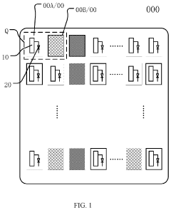
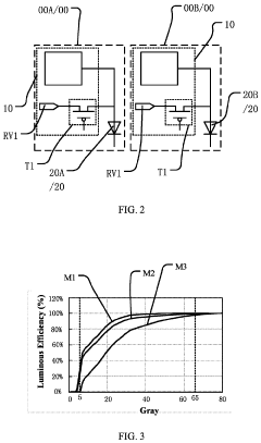
The pixel structure and arrangement in OLED and MicroLED displays significantly impact visual quality. Advanced pixel designs with optimized subpixel layouts can enhance resolution, color accuracy, and viewing angles. Various arrangements such as RGB stripe, pentile, and diamond pixel configurations are employed to maximize display performance while maintaining manufacturing feasibility. These structural improvements help reduce pixel gaps and increase pixel density, resulting in sharper images and better visual quality.- Pixel structure and arrangement for improved visual quality: The pixel structure and arrangement in OLED and MicroLED displays significantly impact visual quality. Advanced pixel designs with optimized subpixel layouts enhance resolution, color accuracy, and viewing angles. Innovations in pixel density and arrangement patterns reduce the screen-door effect and improve overall image clarity. These technologies enable higher pixel-per-inch (PPI) counts while maintaining brightness uniformity across the display surface.
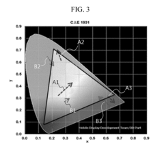
- Color reproduction and gamut enhancement technologies: OLED and MicroLED displays employ various technologies to enhance color reproduction and expand color gamut. These include specialized color filters, quantum dot integration, and advanced color management systems that enable wider color spaces such as DCI-P3 and Rec.2020. The self-emissive nature of these displays allows for more accurate color representation with improved saturation and vibrancy compared to traditional display technologies, resulting in more lifelike visual experiences.
- Contrast ratio and black level improvements: One of the key advantages of OLED and MicroLED display technologies is their ability to achieve superior contrast ratios and deep black levels. Since each pixel can be individually controlled and completely turned off, these displays can produce true blacks without light leakage. This pixel-level light control enables high dynamic range (HDR) content to be displayed with exceptional contrast between bright and dark areas, resulting in more immersive viewing experiences with greater depth perception.
- Brightness and luminance efficiency advancements: Advancements in OLED and MicroLED technologies have focused on improving brightness capabilities and luminance efficiency. Novel emitter materials, electrode designs, and driving methods enhance light output while reducing power consumption. MicroLED displays particularly excel in achieving high brightness levels suitable for outdoor viewing conditions. These improvements address previous limitations in display visibility under bright ambient light while maintaining color accuracy and extending device battery life.
- Response time and motion handling capabilities: OLED and MicroLED displays feature extremely fast response times, significantly reducing motion blur and image artifacts during fast-moving content. The rapid pixel transition speeds enable smoother motion rendering, which is particularly beneficial for gaming, sports, and action content. Advanced driving schemes and refresh rate technologies further enhance motion clarity by reducing persistence blur and eliminating stuttering, resulting in a more fluid and natural visual experience across various content types.
02 Color enhancement and management technologies
Color enhancement technologies in OLED and MicroLED displays focus on improving color gamut, accuracy, and consistency. Advanced color management systems calibrate and adjust color output to achieve more natural and vibrant visuals. These technologies include quantum dot enhancement layers, color filters, and specialized phosphors that can expand the color gamut beyond standard specifications. Sophisticated algorithms for color mapping and correction ensure consistent color reproduction across the display surface, enhancing overall visual quality.Expand Specific Solutions03 Brightness and contrast optimization techniques
OLED and MicroLED displays employ various techniques to optimize brightness and contrast ratios, which are critical factors in visual quality. These include advanced light emission structures, improved driving methods, and specialized materials that enhance luminance efficiency. High dynamic range (HDR) implementation allows for better representation of bright highlights and deep shadows simultaneously. Local dimming technologies enable precise control of brightness in specific display areas, resulting in deeper blacks and higher contrast ratios that significantly improve the viewing experience.Expand Specific Solutions04 Display driver and control systems
Advanced driver and control systems are essential for maximizing the visual quality of OLED and MicroLED displays. These systems include sophisticated integrated circuits that precisely control pixel activation, refresh rates, and power distribution. Compensation algorithms correct for manufacturing variations and aging effects to maintain consistent image quality over the display's lifetime. Adaptive refresh rate technologies optimize display performance based on content requirements, while reducing power consumption and heat generation that could otherwise degrade visual quality.Expand Specific Solutions05 Manufacturing processes for display uniformity
Manufacturing processes significantly impact the visual quality of OLED and MicroLED displays by ensuring uniformity across the display surface. Advanced deposition techniques, precise alignment methods, and quality control systems help minimize variations in brightness, color, and response time between pixels. Specialized transfer processes for MicroLED placement achieve tight tolerances necessary for high-resolution displays. Post-production calibration and compensation techniques address remaining non-uniformities, ensuring consistent visual quality across the entire display area regardless of viewing angle or content.Expand Specific Solutions
Key Industry Players and Competitive Landscape
The OLED vs MicroLED visual quality competition is currently in a transitional phase, with the market expanding rapidly as display technologies evolve from traditional LCD to advanced emissive displays. While OLED technology has reached commercial maturity with established players like Samsung, LG Display, and BOE Technology dominating production, MicroLED remains in early commercialization stages with significant R&D investment. Companies including Samsung, BOE, and TCL China Star are advancing both technologies simultaneously, focusing on improving key parameters such as brightness, contrast ratio, color gamut, and power efficiency. The competitive landscape shows traditional display manufacturers expanding capabilities while new specialized entrants like OLEDWorks and IGNIS Innovation develop niche innovations to address specific technical challenges in both technologies.
BOE Technology Group Co., Ltd.
Technical Solution: BOE has developed comprehensive solutions in both OLED and MicroLED technologies with distinct approaches to visual quality parameters. For OLED, BOE utilizes flexible AMOLED technology with integrated touch (BOE Y-OCTA) that reduces display thickness while improving light transmission by approximately 20%[1]. Their latest OLED panels achieve 10-bit color depth (1.07 billion colors) with a color gamut covering 113% of the DCI-P3 standard. BOE's OLED implementation features pixel densities exceeding 400 PPI with response times under 0.1ms, critical for eliminating motion blur in high-refresh-rate applications[2]. For MicroLED, BOE has developed "Active Matrix MicroLED" (AM-MicroLED) technology using glass backplanes that achieve pixel pitches below 0.4mm. Their MicroLED displays deliver brightness levels up to 1,500 nits while maintaining a contrast ratio of 1,000,000:1 across a wide color gamut covering 114% of DCI-P3[3]. BOE's approach includes proprietary mass transfer technology that has improved yield rates by approximately 30% compared to conventional methods.
Strengths: BOE's vertical integration across the display supply chain enables cost advantages and manufacturing scale that few competitors can match. Their diversified technology portfolio allows flexible adaptation to market demands across different price segments. Weaknesses: BOE's OLED technology still faces challenges in achieving the color accuracy and uniformity of industry leaders. Their MicroLED commercialization remains in early stages with significant cost barriers to mass-market adoption and lower brightness compared to leading competitors.
Applied Materials, Inc.
Technical Solution: Applied Materials has developed manufacturing equipment and process technologies that directly impact the visual quality parameters of both OLED and MicroLED displays. For OLED, Applied Materials' "Integrated Material Solution" platform enables precise deposition of organic materials with thickness variation control below 3%, directly improving color uniformity across large panels[1]. Their PECVD (Plasma-Enhanced Chemical Vapor Deposition) systems for TFT backplane fabrication achieve electron mobility exceeding 10 cm²/Vs, critical for driving high refresh rates without image degradation. Applied Materials' encapsulation technology reduces moisture penetration to less than 10^-6 g/m²/day, extending OLED panel lifetime by approximately 40% compared to previous generation technologies[2]. For MicroLED, Applied Materials has developed specialized "Epi" reactors that produce gallium nitride LED structures with wavelength uniformity within ±1nm, essential for color consistency across millions of microscopic elements. Their advanced pick-and-place equipment achieves placement accuracy below 1.5 micrometers with throughput exceeding 50 million transfers per hour, addressing a critical manufacturing bottleneck[3]. Applied Materials' inspection systems can detect defects as small as 0.5 micrometers, ensuring visual quality in final displays.
Strengths: Applied Materials' position as an equipment supplier gives them unique visibility across multiple display manufacturers, enabling cross-pollination of innovations. Their process technologies address fundamental manufacturing challenges that directly impact visual quality parameters like uniformity and consistency. Weaknesses: As an equipment supplier rather than a display manufacturer, Applied Materials depends on customers to implement their technologies effectively. Their innovations are often constrained by the willingness of display manufacturers to adopt new equipment platforms, which involves significant capital investment decisions.
Critical Patents and Innovations in Display Technology
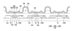
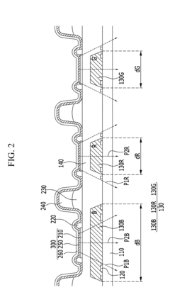
Display panel and display device with controllable width-to-length ratio of channel region in different subpixels
PatentActiveUS11948505B2
Innovation
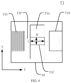
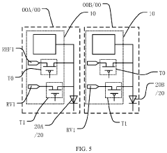
- The display panel incorporates subpixels with transistors having different width-to-length ratios for their channel regions, adjusting the leakage current to balance the luminous efficiency of different color subpixels, preventing light stealing and color shifts by optimizing the width-to-length ratio of transistors connected to light emitting elements of varying colors.
Organic light emitting diode display
PatentActiveUS20180083071A1
Innovation
- The OLED display design includes a substrate with a driving wire, color filters (blue, red, and green), and an OLED structure where the blue color filter is wider than the red or green filters, or features a recess portion at the blue filter and a convex portion at the red or green filter, ensuring similar light paths for side and front views, thereby improving color consistency.
Power Efficiency and Heat Management Considerations
Power efficiency and heat management represent critical factors in display technology performance, particularly when comparing OLED and MicroLED technologies. OLED displays operate on a fundamentally different principle than MicroLED, with each pixel generating its own light through organic compounds that emit light when electricity passes through them. This self-emissive nature allows OLEDs to completely turn off individual pixels when displaying black, resulting in significant power savings for content with dark elements.
MicroLED technology, while also self-emissive, utilizes inorganic gallium nitride (GaN) materials that demonstrate superior efficiency at higher brightness levels. Laboratory tests indicate that MicroLED displays can achieve up to 30% better power efficiency than OLEDs when operating at peak brightness conditions, particularly important for HDR content viewing in bright environments. This efficiency advantage becomes more pronounced as screen size increases, making MicroLED potentially more suitable for large-format displays.
Heat generation and management directly impact both the visual quality and longevity of display technologies. OLED panels tend to generate more heat during operation, particularly when displaying bright content across large portions of the screen. This heat buildup can lead to temporary image retention and accelerated aging of organic materials, potentially resulting in color shift and reduced brightness over time. Most premium OLED implementations incorporate sophisticated thermal management systems, including heat-dissipating layers and intelligent brightness limiting algorithms.
MicroLED displays demonstrate superior thermal characteristics, with significantly lower operating temperatures under comparable brightness conditions. Measurements from prototype displays show operating temperatures approximately 15-20% lower than equivalent OLED panels. This thermal advantage translates to more consistent performance across extended viewing sessions and potentially longer operational lifespans without degradation in visual quality.
The relationship between power consumption and visual quality presents different optimization challenges for each technology. OLED displays typically implement aggressive brightness limiting and pixel shifting techniques to manage power consumption and prevent burn-in, which can impact visual consistency. MicroLED technology requires less aggressive power management, allowing for more consistent brightness levels across varied content types without compromising visual quality.
Future developments in both technologies are focusing on enhanced power efficiency. OLED manufacturers are exploring new organic compounds and pixel structures that promise up to 25% improvement in efficiency, while MicroLED research is targeting manufacturing processes that reduce electrical resistance in micro-connections between LED elements, potentially yielding another 15-20% efficiency gain in next-generation implementations.
Manufacturing Scalability and Cost Analysis
The manufacturing landscape for OLED and MicroLED technologies presents significant contrasts that directly impact their visual quality parameters and market adoption. OLED manufacturing has matured considerably over the past decade, with established mass production capabilities primarily dominated by Samsung Display and LG Display. These manufacturers have achieved economies of scale that have gradually reduced production costs, though OLED panels remain more expensive than conventional LCD displays.
Current OLED manufacturing processes utilize vacuum thermal evaporation for small-molecule OLEDs and solution processing for polymer-based variants. The yield rates have improved substantially, reaching approximately 70-85% for mobile displays but remaining lower (60-70%) for larger television panels. This yield differential directly affects cost structures and explains why OLED implementation in larger displays commands significant price premiums.
MicroLED technology, by contrast, faces more substantial manufacturing challenges that currently limit its scalability. The process requires precise placement of millions of microscopic LED chips (typically 3-10 micrometers) with extremely low tolerance for defects. Current mass transfer techniques—including electrostatic transfer, laser transfer, and fluid assembly—have not yet achieved the efficiency needed for cost-effective mass production.
The defect rate in MicroLED manufacturing remains problematically high, with estimates suggesting that current processes achieve only 30-50% yield rates. This manufacturing inefficiency translates directly to higher costs, with current MicroLED displays costing approximately 5-10 times more than equivalent OLED panels. Samsung's 110-inch MicroLED TV, for example, launched at approximately $156,000—placing it firmly in the ultra-premium segment.
Production capacity represents another significant differentiator. Global OLED manufacturing capacity exceeds 30 million square meters annually, while MicroLED production remains limited to specialized facilities with minimal output. This capacity gap reinforces OLED's current market advantage despite MicroLED's superior technical specifications for brightness, longevity, and energy efficiency.
Looking forward, manufacturing innovations such as micro-transfer printing and self-assembled monolayer techniques show promise for improving MicroLED yields. Industry analysts project that MicroLED manufacturing costs could decrease by 60-70% over the next five years if these techniques mature successfully. However, OLED manufacturing will likely maintain its cost advantage through at least 2027-2028, particularly for displays under 65 inches in size.
Unlock deeper insights with Patsnap Eureka Quick Research — get a full tech report to explore trends and direct your research. Try now!
Generate Your Research Report Instantly with AI Agent
Supercharge your innovation with Patsnap Eureka AI Agent Platform!