

OLED vs MicroLED Influence on Semiconductor Fabrication
OCT 24, 20259 MIN READ
Generate Your Research Report Instantly with AI Agent
Patsnap Eureka helps you evaluate technical feasibility & market potential.
Display Technology Evolution and Objectives
Display technology has undergone remarkable evolution over the past several decades, transitioning from cathode ray tubes (CRTs) to liquid crystal displays (LCDs), and subsequently to organic light-emitting diode (OLED) technology. This progression has been driven by continuous demands for higher resolution, improved energy efficiency, enhanced color accuracy, and reduced form factors. Currently, the industry stands at a pivotal juncture with OLED technology reaching maturity while MicroLED emerges as a promising next-generation display technology.
OLED technology, commercialized in the early 2000s, revolutionized displays by eliminating the need for backlighting, enabling thinner screens with superior contrast ratios and more vibrant colors. The semiconductor fabrication processes for OLED displays involve thin-film transistor (TFT) backplanes, typically utilizing low-temperature polysilicon (LTPS) or indium gallium zinc oxide (IGZO) technologies, followed by the deposition of organic materials through techniques such as vacuum thermal evaporation.
MicroLED technology represents the next evolutionary step, offering potential advantages in brightness, energy efficiency, and longevity. Unlike OLEDs, MicroLEDs utilize inorganic gallium nitride (GaN) based materials, which present fundamentally different semiconductor fabrication challenges. The manufacturing process involves the precise placement of microscopic LED arrays, requiring advanced epitaxial growth techniques and mass transfer technologies that are still evolving.
The semiconductor industry's trajectory is increasingly influenced by these display technologies, as fabrication facilities must adapt to accommodate their unique requirements. For OLED production, semiconductor manufacturers have invested in specialized equipment for organic material deposition and encapsulation. MicroLED manufacturing, however, demands even more precise lithography, etching processes, and novel mass transfer techniques to handle millions of microscopic LED chips.
The primary technical objective in this evolving landscape is to develop semiconductor fabrication processes that can efficiently produce both OLED and MicroLED displays at scale, while continuously improving yield rates and reducing production costs. This includes addressing challenges such as pixel density limitations, color accuracy, and manufacturing complexity.
Looking forward, the industry aims to achieve several critical milestones: reducing MicroLED manufacturing costs to competitive levels, solving mass transfer challenges for microscopic LED elements, improving quantum efficiency of blue MicroLEDs, and developing hybrid approaches that might combine the strengths of both technologies. The ultimate goal is to establish fabrication processes that can deliver next-generation displays with perfect black levels, ultra-high brightness, extended lifespans, and reduced power consumption.
Market Demand Analysis for Advanced Display Technologies
The display technology market is witnessing a significant shift as advanced technologies like OLED and MicroLED continue to evolve. Current market analysis indicates that the global display market is experiencing robust growth, driven primarily by increasing demand for high-resolution, energy-efficient displays across multiple sectors including consumer electronics, automotive, healthcare, and industrial applications.
OLED technology has established a strong market presence, particularly in smartphones and premium televisions. The OLED display market has been expanding at a compound annual growth rate of approximately 15% over the past five years, with smartphone displays accounting for the largest segment. Major smartphone manufacturers have increasingly adopted OLED displays due to their superior color reproduction, contrast ratios, and flexibility.
Meanwhile, MicroLED technology, though still in its early commercialization stages, is generating substantial market interest due to its potential advantages over existing technologies. Market research suggests that the MicroLED segment is poised for explosive growth, with projections indicating a potential market value increase from its current nascent state to a multi-billion dollar industry within the next decade.
Consumer demand for improved visual experiences is a primary driver for both technologies. High dynamic range (HDR), wider color gamut, and higher refresh rates are becoming standard expectations rather than premium features. This trend is particularly evident in gaming displays and high-end televisions, where visual performance directly correlates with consumer purchasing decisions.
The automotive sector represents another rapidly growing market for advanced display technologies. The transition toward electric vehicles and autonomous driving systems has increased the demand for sophisticated in-vehicle displays. OLED technology has gained traction in this sector due to its flexibility and form factor advantages, while MicroLED is being explored for its durability and brightness capabilities essential for automotive applications.
Regional analysis reveals that East Asia continues to dominate the display technology market, both in terms of production and consumption. However, North America and Europe show strong demand growth, particularly in premium segments where technological differentiation commands price premiums.
The semiconductor fabrication implications of these market trends are substantial. As demand for these advanced display technologies grows, there is increasing pressure on semiconductor manufacturers to develop specialized fabrication processes. This market demand is driving innovations in thin-film transistor (TFT) backplanes, epitaxial growth techniques, and mass transfer processes essential for both OLED and MicroLED production.
OLED vs MicroLED: Technical Challenges and Limitations
While OLED technology has matured significantly over the past decade, it still faces several technical limitations. The organic materials used in OLED displays are susceptible to degradation when exposed to oxygen and moisture, resulting in reduced lifespan compared to inorganic alternatives. This degradation manifests as color shifting and reduced brightness over time, particularly affecting blue OLED elements which typically degrade faster than red and green counterparts. Manufacturing challenges persist in achieving consistent yields at scale, especially for larger display sizes where defect rates increase exponentially.
From a semiconductor fabrication perspective, OLED production requires precise deposition of multiple organic layers with thicknesses measured in nanometers, demanding extremely tight process controls. The low-temperature polysilicon (LTPS) backplanes commonly used for OLED displays require complex manufacturing processes that limit production capacity and increase costs.
MicroLED technology, while promising superior performance, faces even more significant manufacturing hurdles. The primary challenge lies in the mass transfer process - moving millions of microscopic LED chips from their growth substrate to the display backplane with near-perfect yield. Current pick-and-place technologies struggle to achieve the necessary throughput and precision for commercial viability at competitive price points.
The semiconductor fabrication requirements for MicroLED are particularly demanding, requiring integration of III-V compound semiconductor materials (typically gallium nitride) with silicon backplanes. This heterogeneous integration presents significant challenges in thermal management and stress handling due to coefficient of thermal expansion mismatches between materials.
Defect management represents another critical limitation for MicroLED. With millions of individual LEDs in a single display, even a 99.9999% yield would result in hundreds of defective pixels, necessitating redundancy schemes and repair mechanisms that further complicate the manufacturing process.
Color conversion techniques for MicroLED displays present additional challenges. While blue MicroLEDs have achieved reasonable efficiency, producing red and green through phosphor or quantum dot conversion layers introduces complexity and potential efficiency losses. Direct-emission red and green MicroLEDs remain less efficient than their blue counterparts.
Both technologies face scaling challenges in opposite directions. OLED struggles with scaling to very large displays while maintaining yield, whereas MicroLED faces difficulties scaling down to smartphone-sized pixel densities while preserving manufacturing economics. These complementary limitations have created distinct market segments where each technology currently holds advantages.
Current Semiconductor Fabrication Solutions for OLED and MicroLED
01 OLED device structure and fabrication methods
Organic Light Emitting Diode (OLED) technology involves specific device structures and fabrication methods to achieve optimal display performance. These include multilayer structures with organic emissive layers sandwiched between electrodes, specialized deposition techniques for organic materials, and encapsulation methods to protect sensitive organic components from environmental degradation. Advanced OLED fabrication also incorporates thin-film transistor (TFT) backplanes for active matrix control and various approaches to improve efficiency and lifetime of the devices.- OLED device structure and fabrication methods: Organic Light Emitting Diode (OLED) technology involves specific device structures and fabrication methods for display applications. These include multilayer structures with organic emissive layers sandwiched between electrodes, various deposition techniques for organic materials, and encapsulation methods to protect against environmental degradation. Advanced OLED fabrication processes focus on improving efficiency, lifetime, and display quality through innovations in materials science and semiconductor processing techniques.
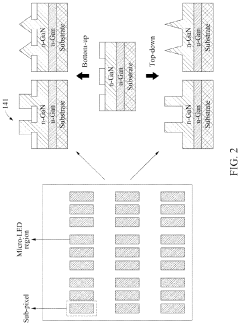
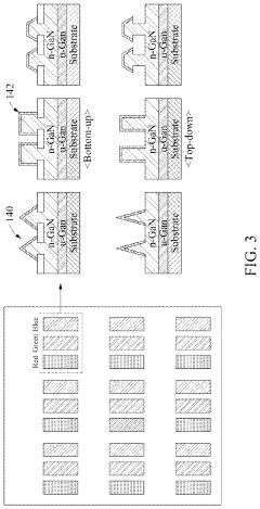
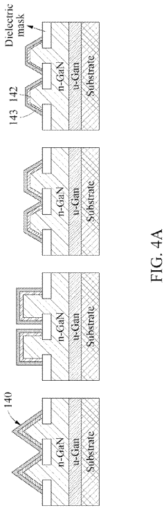
- MicroLED fabrication and integration technologies: MicroLED display technology utilizes microscopic LED arrays that require specialized fabrication and integration methods. The manufacturing process involves epitaxial growth of LED structures, transfer techniques to position micro-scale LEDs onto display substrates, and integration with driving circuits. Key challenges addressed in these patents include mass transfer processes, pixel alignment, and electrical interconnection methods that enable high-resolution, high-brightness display applications with improved energy efficiency.
- Semiconductor backplane technologies for displays: Advanced semiconductor backplanes are essential for driving both OLED and MicroLED displays. These technologies include thin-film transistor (TFT) arrays using various semiconductor materials such as silicon, oxide semiconductors, or organic semiconductors. The backplane designs focus on improving pixel driving capabilities, reducing power consumption, and enabling high refresh rates. Integration methods between the semiconductor backplane and the emissive elements are critical for display performance and manufacturing yield.
- Color conversion and quantum dot technologies: Color conversion technologies enhance display performance in both OLED and MicroLED applications. These include quantum dot materials that convert light from blue or UV emitters to precise color wavelengths, color filters, and phosphor-based conversion layers. The integration of these materials improves color gamut, brightness, and energy efficiency of displays while simplifying the manufacturing process by potentially reducing the need for separate red, green, and blue emitter fabrication.
- Display module integration and packaging techniques: Integration and packaging technologies are crucial for the final assembly of display modules using OLED or MicroLED technologies. These include methods for flexible and foldable display fabrication, bezel-less design approaches, and techniques for integrating touch functionality. Advanced packaging solutions address thermal management, mechanical durability, and optical performance optimization. The patents also cover modular display designs that allow for scalable screen sizes and novel form factors for various applications.
02 MicroLED fabrication and integration techniques
MicroLED display technology relies on microscopic inorganic LED arrays that require specialized fabrication and integration techniques. These include epitaxial growth of LED structures, mass transfer methods to position tiny LED chips onto display substrates, and integration with driving circuits. The fabrication process involves semiconductor processing techniques such as photolithography, etching, and metallization to create the microscopic LED structures, followed by innovative approaches to handle and place these tiny components with high precision and yield.Expand Specific Solutions03 Pixel architecture and driving methods for advanced displays
Advanced pixel architectures and driving methods are crucial for both OLED and MicroLED displays. These include sub-pixel arrangements for color reproduction, compensation circuits to address uniformity issues, and various driving schemes to control brightness and color accuracy. The pixel designs incorporate transistor configurations for stable current delivery, storage capacitors for frame retention, and specialized circuit layouts to minimize power consumption while maximizing display performance. Novel driving methods also address issues like motion blur and image retention.Expand Specific Solutions04 Semiconductor materials and quantum dot integration
Semiconductor materials play a critical role in both OLED and MicroLED technologies, with recent innovations focusing on quantum dot integration. These materials include specialized semiconductors for light emission, quantum dots for color conversion and enhancement, and novel composite materials that improve efficiency and color gamut. The fabrication processes involve precise control of material composition, doping profiles, and interface engineering to achieve desired optoelectronic properties. Quantum dot integration enables improved color performance through down-conversion of blue or UV light to precise wavelengths.Expand Specific Solutions05 Manufacturing processes and equipment for display production
Manufacturing processes and specialized equipment are essential for mass production of OLED and MicroLED displays. These include vacuum deposition systems, lithography equipment, inspection tools, and automated assembly lines. Advanced manufacturing techniques involve roll-to-roll processing for flexible displays, laser processing for precise patterning, and specialized bonding methods for component integration. Quality control systems and yield management strategies are also critical aspects of the manufacturing process, incorporating in-line testing and repair capabilities to ensure cost-effective production of high-performance displays.Expand Specific Solutions
Key Industry Players in Display Manufacturing
The OLED vs MicroLED competition in semiconductor fabrication is currently in a transitional phase, with OLED technology reaching maturity while MicroLED remains in early commercialization. The global market for these display technologies is projected to exceed $200 billion by 2025, driven by consumer electronics and automotive applications. Established players like Samsung Display, LG Electronics, and BOE Technology dominate OLED production with mature manufacturing processes, while MicroLED development is led by companies including Apple, Samsung, and specialized firms like Chengdu Vistar Optoelectronics. Equipment suppliers such as Applied Materials are positioned strategically across both technologies. The technical challenges for MicroLED mass production remain significant, particularly in mass transfer techniques and yield management, creating opportunities for semiconductor fabrication innovation from companies like SMIC and Intel.
BOE Technology Group Co., Ltd.
Technical Solution: BOE has developed comprehensive semiconductor fabrication approaches for both OLED and MicroLED technologies. For OLED, BOE employs LTPO (Low-Temperature Polycrystalline Oxide) backplane technology in their advanced fabs, which enables variable refresh rates and lower power consumption. Their OLED fabrication process utilizes vacuum evaporation with shadow masks for RGB patterning and incorporates advanced thin film encapsulation (TFE) techniques. For MicroLED, BOE has invested in a hybrid approach combining traditional semiconductor fabrication with novel mass transfer methods. Their process involves epitaxial growth of GaN-based LED structures, followed by wafer-level processing and a proprietary "micro-fluidic assembly" technique for transferring and placing microscopic LED chips onto TFT substrates. BOE has also developed specialized semiconductor testing protocols to identify defective MicroLED pixels before final assembly, significantly improving manufacturing yields.
Strengths: Extensive Gen 6 and Gen 8.5 fab capacity; strong government backing for semiconductor development; vertical integration from materials to modules; advanced LTPO backplane technology. Weaknesses: Still catching up to Korean manufacturers in OLED yield rates; MicroLED mass production capabilities remain limited; higher defect rates in larger display applications.
LG Electronics, Inc.
Technical Solution: LG has established distinctive semiconductor fabrication approaches for both OLED and MicroLED technologies. For OLED, LG utilizes white OLED (WOLED) technology with color filters, which differs significantly from Samsung's RGB direct emission approach. This fabrication method involves depositing multiple organic layers that together produce white light, followed by color filtering. The process requires fewer mask steps in semiconductor fabrication compared to RGB OLED, enabling larger substrate sizes and higher yields for large displays. For MicroLED, LG has developed a proprietary "monolithic integration" approach that aims to fabricate MicroLED arrays directly on semiconductor wafers without requiring mass transfer. This involves GaN-on-silicon epitaxy processes and specialized wafer bonding techniques to integrate the LED structure with driving circuitry. LG has also pioneered advanced semiconductor packaging solutions for MicroLED, including chip-on-board (COB) technologies that improve thermal management and reliability.
Strengths: Industry-leading WOLED technology for large displays; advanced TFT backplane fabrication capabilities; innovative monolithic MicroLED approach reduces assembly complexity; strong vertical integration. Weaknesses: WOLED technology has lower color volume than RGB approaches; MicroLED monolithic integration faces scaling challenges; higher power consumption in certain OLED implementations.
Critical Patents and Innovations in Display Manufacturing
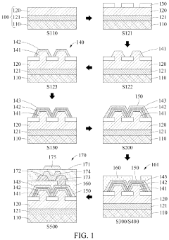
Method of manufacturing micro-light emitting diode-based display and micro-light emitting diode-based display
PatentActiveUS20210143299A1
Innovation
- A method is developed to form multi-wavelength micro-LEDs on a single substrate using a single process, integrating a thin-film transistor (TFT) without a transferring process, allowing for the creation of a 3D light emitting structure and a current spreading layer to enable active operation and full-color display.
Element transfer device and element transfer method
PatentPendingUS20220262665A1
Innovation
- An element transfer device with an elastic sheet and pickup portions, including a shaft portion and head portions, that can adjust its distance between pickup points to match the spacing on both the element and circuit substrates, allowing for simultaneous transfer of multiple micro LEDs.
Supply Chain Implications for Semiconductor Materials
The transition from OLED to MicroLED technologies is creating significant ripple effects throughout semiconductor material supply chains. Traditional OLED production relies heavily on organic compounds and specialized glass substrates, while MicroLED fabrication demands ultra-pure semiconductor materials and more complex epitaxial growth processes. This fundamental difference is reshaping material sourcing strategies across the industry.
For semiconductor manufacturers, MicroLED's stringent requirements for gallium nitride (GaN), indium gallium nitride (InGaN), and other III-V compound semiconductors are creating new bottlenecks. These materials face supply constraints due to limited production capacity and geographic concentration of mining operations, particularly for rare earth elements essential to phosphor development. Material purity requirements for MicroLED are substantially higher than for OLED, necessitating advanced purification technologies and more sophisticated quality control systems.
The geographical distribution of material suppliers is also shifting dramatically. While OLED material production has been concentrated in East Asia, particularly South Korea and Japan, MicroLED's reliance on specialized semiconductor materials is creating opportunities for suppliers in North America and Europe with advanced material science capabilities. This redistribution may help mitigate some supply chain vulnerabilities but introduces new logistical challenges.
Recycling and material recovery processes are becoming increasingly important as both technologies utilize rare and expensive materials. MicroLED's longer theoretical lifespan could reduce material consumption over time, but its complex material composition presents greater recycling challenges compared to OLED's simpler organic structure. This is prompting investment in advanced material recovery technologies specifically designed for next-generation display components.
Price volatility remains a critical concern, particularly for MicroLED materials. The limited supplier base for specialized materials like quantum dots and high-purity GaN substrates creates vulnerability to supply disruptions. Manufacturers are responding by implementing strategic stockpiling programs and developing alternative material formulations to reduce dependency on constrained resources.
Vertical integration strategies are gaining prominence as display manufacturers seek to secure reliable material supplies. Companies like Samsung and Apple are increasingly investing in material production capabilities or forming exclusive partnerships with key suppliers to ensure consistent access to critical components. This trend is accelerating consolidation within the semiconductor materials sector, potentially raising barriers to entry for smaller display manufacturers.
Environmental Impact and Sustainability Considerations
The environmental footprint of display technologies has become increasingly significant as consumer electronics proliferate globally. OLED and MicroLED technologies present distinct environmental challenges and opportunities throughout their lifecycle, from raw material extraction to end-of-life disposal, with substantial implications for semiconductor fabrication processes.
OLED manufacturing typically involves fewer process steps than traditional LCD production, potentially reducing energy consumption during fabrication. However, the organic materials in OLEDs often require rare elements and specialized chemicals that present extraction and disposal challenges. The semiconductor fabrication processes for OLED backplanes utilize toxic gases and solvents that necessitate comprehensive waste management systems, contributing to the technology's environmental burden.
MicroLED manufacturing, while still evolving, demonstrates promising sustainability advantages. The inorganic nature of MicroLEDs eliminates the need for many environmentally problematic organic compounds. However, the current mass transfer processes for MicroLED production can be energy-intensive and yield-challenged, potentially offsetting some environmental benefits. The extremely precise semiconductor fabrication requirements also demand significant clean room resources and ultrapure water usage.
Energy efficiency during operation represents a critical sustainability factor. MicroLEDs demonstrate superior energy efficiency compared to OLEDs, particularly at high brightness levels, potentially reducing the carbon footprint during the product use phase. This operational efficiency advantage may compensate for higher initial manufacturing impacts, especially for applications with extended usage periods.
Resource utilization differs significantly between technologies. OLED production has benefited from years of process optimization, resulting in more efficient material usage. MicroLED fabrication currently faces yield challenges that can lead to material waste, though technological improvements are rapidly addressing this issue. Both technologies require specialized semiconductor fabrication equipment that embodies significant embedded energy and resources.
End-of-life considerations reveal further distinctions. OLEDs contain organic materials that may present recycling challenges, while MicroLEDs primarily comprise inorganic materials that could potentially be more recyclable. However, both technologies incorporate semiconductor components with precious metals and rare elements that warrant recovery systems to minimize resource depletion.
Water usage in semiconductor fabrication for both technologies remains a significant environmental concern. OLED and MicroLED manufacturing facilities typically require millions of gallons of ultrapure water daily, with varying levels of contamination in wastewater that necessitate extensive treatment before release. Innovations in water recycling systems and dry processing techniques are gradually reducing this impact across the industry.
Unlock deeper insights with Patsnap Eureka Quick Research — get a full tech report to explore trends and direct your research. Try now!
Generate Your Research Report Instantly with AI Agent
Supercharge your innovation with Patsnap Eureka AI Agent Platform!