OLED vs MicroLED: Bridging the Gap in Optical Technology
OCT 24, 20259 MIN READ
Generate Your Research Report Instantly with AI Agent
Patsnap Eureka helps you evaluate technical feasibility & market potential.
OLED and MicroLED Technology Evolution and Objectives
The evolution of display technologies has witnessed significant advancements over the past decades, with OLED (Organic Light-Emitting Diode) and MicroLED emerging as pivotal innovations in the optical technology landscape. OLED technology, first conceptualized in the 1950s, saw practical development in the 1980s by Eastman Kodak, with commercial applications beginning in the early 2000s. The technology has since evolved from passive-matrix to active-matrix configurations, enabling higher resolution and improved energy efficiency.
MicroLED represents a more recent technological advancement, with foundational research beginning in the early 2000s. Unlike OLED, which utilizes organic compounds, MicroLED employs inorganic gallium nitride-based materials to create self-emissive displays. This fundamental difference has positioned MicroLED as a potential successor to OLED in various applications, particularly where brightness, longevity, and energy efficiency are paramount.
The technological trajectory of both OLED and MicroLED has been characterized by continuous improvements in manufacturing processes, material science, and integration capabilities. OLED has progressed from simple monochrome displays to flexible, transparent, and even rollable configurations. Meanwhile, MicroLED development has focused on overcoming mass production challenges, particularly in the miniaturization and transfer of millions of microscopic LEDs.
Current industry objectives for OLED technology include enhancing lifetime performance, reducing blue pixel degradation, improving manufacturing yields, and decreasing production costs. For MicroLED, primary objectives revolve around scaling manufacturing processes, improving transfer techniques for micro-scale components, enhancing yield rates, and reducing the significant cost barriers that currently limit widespread adoption.
The convergence point between these technologies presents intriguing possibilities. Hybrid approaches, such as QLED-OLED combinations and MicroLED-enhanced OLED displays, are being explored to leverage the strengths of each technology while mitigating their respective limitations. These hybrid solutions aim to bridge the existing performance gap between the two technologies.
Looking forward, the technological roadmap for both OLED and MicroLED indicates a focus on sustainability, with reduced energy consumption and environmentally friendly manufacturing processes becoming increasingly important. Additionally, integration with emerging technologies such as quantum dots, advanced AI-driven display management, and novel form factors represents the next frontier in display technology evolution.
The ultimate objective for both technologies remains the creation of displays that offer perfect color reproduction, infinite contrast ratios, maximum energy efficiency, extended lifespans, and manufacturing scalability—all at commercially viable price points. The ongoing technological competition between OLED and MicroLED continues to drive innovation toward these ambitious goals.
Display Market Demand Analysis and Trends
The display technology market has witnessed significant growth over the past decade, driven by increasing consumer demand for high-quality visual experiences across various devices. The global display market was valued at approximately $148 billion in 2022 and is projected to reach $206 billion by 2028, representing a compound annual growth rate (CAGR) of 5.7%. This growth trajectory is primarily fueled by the expanding smartphone, television, and wearable device segments.
Consumer preferences are increasingly shifting toward displays with higher resolution, better color accuracy, improved energy efficiency, and innovative form factors. OLED technology has gained substantial market share due to its superior contrast ratios, flexible display capabilities, and thinner profiles compared to traditional LCD displays. The OLED display market reached $38.4 billion in 2022 and continues to grow steadily, particularly in premium smartphones and high-end televisions.
Meanwhile, MicroLED technology is emerging as a promising contender in the high-end display segment. Although currently representing less than 1% of the overall display market, MicroLED is attracting significant investment due to its potential advantages in brightness, longevity, and energy efficiency. Market analysts predict that MicroLED displays could capture 15% of the premium display market by 2030, particularly in applications requiring exceptional brightness and durability.
Regional analysis reveals that Asia-Pacific dominates the display manufacturing landscape, with South Korea, China, and Taiwan collectively accounting for over 70% of global production capacity. However, North America and Europe lead in display technology innovation and premium market segments, particularly for specialized applications in automotive, medical, and aerospace industries.
Industry trends indicate a growing demand for environmentally sustainable display technologies with reduced energy consumption and improved recyclability. This trend aligns with both OLED and MicroLED development roadmaps, as both technologies offer potential advantages in power efficiency compared to traditional LCD displays.
The automotive sector represents one of the fastest-growing segments for advanced display technologies, with a projected CAGR of 12.3% through 2028. The increasing integration of digital cockpits, heads-up displays, and infotainment systems is creating new opportunities for both OLED and MicroLED technologies, with particular emphasis on durability, brightness, and operational temperature range.
Consumer electronics remains the largest application segment, accounting for approximately 65% of display technology demand. Within this segment, smartphones represent the single largest category, followed by televisions and tablets. The growing adoption of wearable devices, including smartwatches and augmented reality headsets, is creating new demand for compact, energy-efficient display solutions that both OLED and emerging MicroLED technologies are positioned to address.
Current Technical Limitations and Development Challenges
Despite significant advancements in both OLED and MicroLED technologies, several critical limitations and challenges persist that hinder their widespread adoption and performance optimization. OLED technology, while commercially established, continues to struggle with limited operational lifespan, particularly for blue emitters which typically degrade faster than red and green counterparts. This differential aging leads to color shift over time, compromising display quality and consistency.
Manufacturing scalability remains a significant hurdle for both technologies. OLED production faces yield challenges at larger screen sizes, while MicroLED confronts even more severe mass production barriers due to the complexity of transferring millions of microscopic LED chips with near-perfect precision. Current transfer techniques achieve approximately 99.99% accuracy, but even this minimal defect rate translates to thousands of defective pixels in a 4K display.
Energy efficiency presents another critical challenge. While both technologies offer improvements over traditional LCD displays, MicroLED theoretically provides superior power efficiency. However, practical implementations have yet to fully realize this potential due to electrical and optical losses in current designs. OLED displays continue to face power consumption issues, especially when displaying bright content.
Material stability constitutes a fundamental limitation for OLED technology. Organic materials are inherently susceptible to degradation from oxygen, moisture, and prolonged high-brightness operation. Despite encapsulation advancements, this vulnerability remains a significant concern for long-term reliability, particularly in professional and automotive applications where extended durability is essential.
For MicroLED, miniaturization presents formidable technical barriers. As pixel sizes decrease below 10 micrometers, quantum efficiency drops dramatically due to increased surface defects relative to volume. Additionally, achieving consistent performance across millions of individual LEDs requires unprecedented manufacturing precision and quality control measures that current production systems struggle to deliver cost-effectively.
Cost structures represent perhaps the most immediate obstacle to market penetration. OLED manufacturing has benefited from years of optimization but remains expensive compared to LCD technology. MicroLED production costs are substantially higher, with estimates suggesting current manufacturing expenses at 5-10 times that of comparable OLED displays, primarily due to complex assembly processes and low yields.
Thermal management challenges affect both technologies differently. OLEDs generate less heat but are more sensitive to temperature fluctuations, while MicroLEDs produce more concentrated heat that requires sophisticated dissipation solutions, particularly in high-brightness applications like automotive displays or outdoor signage.
Current Implementation Solutions and Approaches
01 Emission and light extraction efficiency differences
OLED and MicroLED technologies have fundamental differences in their light emission mechanisms and extraction efficiencies. OLEDs emit light through organic materials that can suffer from internal quantum efficiency limitations, while MicroLEDs utilize inorganic semiconductor materials with potentially higher external quantum efficiency. The gap between these technologies is particularly evident in the way light is generated and extracted from the device structure, affecting overall brightness and power consumption.- Emission and light extraction efficiency differences: OLED and MicroLED technologies differ significantly in their light emission mechanisms and extraction efficiencies. OLEDs emit light through organic materials that often suffer from internal reflection and waveguide effects, limiting extraction efficiency. MicroLEDs, based on inorganic semiconductor materials, typically achieve higher external quantum efficiency and brightness. The gap between these technologies involves optimizing light extraction structures, reducing optical losses, and enhancing directional emission properties.
- Pixel structure and miniaturization challenges: The optical technology gap between OLED and MicroLED relates to their different pixel architectures and miniaturization capabilities. MicroLEDs face challenges in maintaining efficiency when scaled down to microscopic dimensions, particularly with color conversion and light distribution. OLEDs have established sub-pixel structures but struggle with lifetime and brightness at small scales. These differences affect display resolution, color gamut, and optical performance in high-density applications.
- Color conversion and spectrum management: A significant technology gap exists in how OLED and MicroLED displays manage color spectrum and conversion. MicroLEDs typically rely on blue or UV LED chips with phosphor or quantum dot color converters, while OLEDs can directly emit different colors through various organic materials. This fundamental difference creates challenges in color accuracy, gamut coverage, and spectral purity. Advanced optical films and color conversion layers are being developed to bridge this gap and optimize the spectral characteristics of both technologies.
- Optical integration and manufacturing processes: The manufacturing processes and optical integration methods differ substantially between OLED and MicroLED technologies. MicroLEDs require precise transfer and placement techniques for the tiny LED chips, along with specialized optical structures for each emitter. OLEDs use layer deposition processes that create inherently different optical interfaces and light distribution patterns. This technology gap affects production scalability, yield rates, and the implementation of advanced optical features like lensing and waveguides.
- Viewing angle and optical performance stability: OLED and MicroLED technologies exhibit different characteristics in viewing angle performance and optical stability over time. OLEDs typically offer wider viewing angles but may suffer from color shifts and brightness degradation. MicroLEDs generally maintain better brightness and color consistency across viewing angles but require specialized optical films and structures to optimize light distribution. The technology gap involves developing solutions that provide consistent optical performance across different viewing conditions while maintaining efficiency and longevity.
02 Color gamut and spectral performance comparison
A significant technological gap exists between OLED and MicroLED displays in terms of color reproduction capabilities. MicroLEDs typically offer narrower emission spectra resulting in wider color gamuts and more saturated colors compared to OLEDs. This difference stems from the direct-emission nature of inorganic LED materials versus the broader spectral characteristics of organic emitters in OLEDs, impacting color accuracy and display performance in various lighting conditions.Expand Specific Solutions03 Pixel density and miniaturization challenges
The technological gap between OLED and MicroLED displays is evident in their different approaches to pixel miniaturization. While OLEDs can be manufactured with relatively small pixel sizes using established processes, MicroLEDs face significant challenges in mass transfer and yield during the manufacturing of microscopic LED elements. This gap affects the ability to produce high-resolution displays, particularly for small form factors where pixel density is crucial for image quality.Expand Specific Solutions04 Lifetime and degradation characteristics
OLED and MicroLED technologies exhibit different degradation patterns and operational lifetimes. OLEDs typically suffer from organic material degradation over time, especially in blue emitters, leading to color shift and reduced brightness. MicroLEDs generally offer superior lifetime characteristics due to their inorganic semiconductor composition, but may face different reliability challenges related to the miniaturization of inorganic LED structures and their electrical connections.Expand Specific Solutions05 Manufacturing processes and scalability differences
A significant gap exists in the manufacturing approaches for OLED and MicroLED technologies. OLEDs can be produced using established thin-film deposition techniques on large substrates, while MicroLEDs require precise transfer of microscopic LED chips from growth substrates to display backplanes. This fundamental difference creates challenges in scaling MicroLED production to match OLED's manufacturing efficiency, affecting cost structures and market adoption timelines for these competing display technologies.Expand Specific Solutions
Key Industry Players and Competitive Landscape
The OLED vs MicroLED display technology landscape is currently in a transitional phase, with OLED being mature and commercially established while MicroLED remains in early commercialization. The global market for these advanced display technologies is projected to exceed $200 billion by 2025, driven by demand for higher performance displays in consumer electronics, automotive, and commercial applications. In terms of technical maturity, companies like Samsung Electronics and BOE Technology have achieved mass production capability for OLED, while MicroLED development is being actively pursued by Samsung, TCL China Star Optoelectronics, and BOE, though with significant manufacturing challenges. Universal Display Corporation and Lumileds are advancing materials science for both technologies, while Applied Materials is developing critical manufacturing equipment to bridge the production gap between these competing display solutions.
BOE Technology Group Co., Ltd.
Technical Solution: BOE has developed a comprehensive approach to bridging OLED and MicroLED technologies through their "Active Matrix" architecture that can be applied to both display types. For OLED, BOE utilizes flexible AMOLED technology with integrated touch sensors and under-display fingerprint recognition. Their OLED displays feature pixel densities exceeding 400 PPI with 100% DCI-P3 color gamut coverage. For MicroLED, BOE has created a proprietary "chip-on-glass" process that directly bonds micro-sized LED chips to glass substrates without requiring traditional packaging. This reduces the minimum LED size to under 50 micrometers while improving thermal management. BOE's hybrid approach involves implementing quantum dot color conversion layers with blue MicroLEDs, similar to Samsung's strategy but with proprietary manufacturing processes[2]. BOE has also developed a unique "printing transfer" technique for MicroLED mass production that can place thousands of MicroLED chips simultaneously, potentially reducing manufacturing costs by up to 60% compared to traditional pick-and-place methods.
Strengths: BOE's massive production capacity allows for economies of scale in both technologies. Their printing transfer technique shows promise for cost reduction in MicroLED manufacturing. Strong R&D capabilities with over 10,000 patents in display technologies. Weaknesses: Still catching up to Samsung and LG in high-end OLED manufacturing quality. Their MicroLED technology remains primarily in the prototype stage for consumer applications, with limited commercial deployment.
Samsung Electronics Co., Ltd.
Technical Solution: Samsung has pioneered both OLED and MicroLED technologies with significant advancements in bridging the gap between them. Their OLED technology utilizes organic compounds that emit light when electricity is applied, achieving perfect blacks and high contrast ratios. For MicroLED, Samsung has developed "The Wall" - a modular MicroLED display system using inorganic gallium nitride-based LEDs smaller than 100 micrometers. Samsung's hybrid approach involves implementing quantum dot color conversion layers with blue MicroLEDs to achieve superior color performance while maintaining MicroLED's longevity benefits. Their manufacturing process includes a mass transfer technique that places millions of microscopic LEDs precisely onto substrates, significantly improving production efficiency[1]. Samsung has also developed specialized driver ICs that can individually control each MicroLED pixel, enabling HDR performance exceeding 2,000 nits while maintaining energy efficiency.
Strengths: Samsung possesses comprehensive intellectual property in both technologies, allowing for strategic development of hybrid solutions. Their vertical integration from semiconductor manufacturing to display production creates supply chain advantages. Their modular MicroLED approach offers scalability advantages. Weaknesses: High manufacturing costs for MicroLED technology limit mass-market adoption. The mass transfer process for MicroLEDs still faces yield challenges at consumer electronics scales.
Core Patents and Technical Innovations Analysis
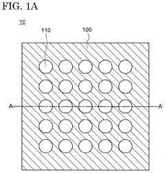
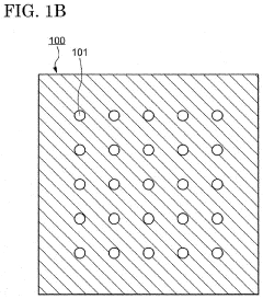
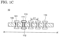
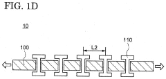
Element transfer device and element transfer method
PatentPendingUS20220262665A1
Innovation
- An element transfer device with an elastic sheet and pickup portions, including a shaft portion and head portions, that can adjust its distance between pickup points to match the spacing on both the element and circuit substrates, allowing for simultaneous transfer of multiple micro LEDs.
LED display and electronic device having same
PatentWO2019208919A1
Innovation
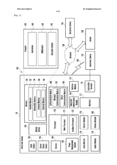
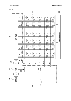
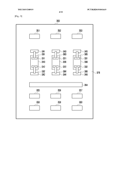
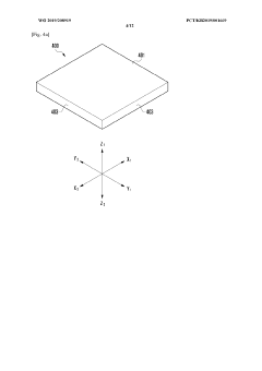
- The development of a micro-LED display with a bezel-less design and segmentation capabilities, allowing for flexible displays of various sizes, achieved through direct mounting of micro-LEDs on a substrate and innovative electrical connections using conductive patterns and wiring lines, enabling robust electrical connections and flexible display configurations.
Manufacturing Process Comparison and Scalability
The manufacturing processes for OLED and MicroLED technologies represent a critical differentiator in their commercial viability and market adoption. OLED manufacturing has matured significantly over the past decade, with established production methods including vacuum thermal evaporation for small molecule OLEDs and solution processing for polymer-based variants. These processes have been refined to achieve reasonable yields at scale, particularly for smaller display applications, though challenges persist with larger panel production.
In contrast, MicroLED manufacturing remains in its nascent stages, facing substantial hurdles in mass production. The primary challenge lies in the mass transfer process - moving millions of tiny LED chips from growth substrates to display backplanes with near-perfect precision. Current approaches include pick-and-place methods, laser transfer, and fluid assembly techniques, each with distinct advantages and limitations regarding throughput, accuracy, and scalability.
Yield management presents another significant disparity between these technologies. OLED manufacturing has achieved acceptable defect rates through process optimization, though still struggles with consistency in larger panels. MicroLED production currently experiences much higher defect rates, with each transfer step introducing potential failure points. The microscopic size of MicroLED elements (typically 3-10 microns) demands unprecedented precision in handling and placement.
Cost structures differ markedly between the two technologies. OLED manufacturing benefits from economies of scale and established supply chains, though still requires significant capital investment for production facilities. MicroLED manufacturing currently demands substantially higher investment due to specialized equipment requirements and lower yields. Industry analysts estimate that MicroLED production costs remain 5-10 times higher than OLED for comparable display sizes.
Scalability trajectories show divergent paths. OLED technology has successfully scaled from small smartphone displays to television-sized panels, though with diminishing yield rates at larger sizes. MicroLED faces more fundamental scaling challenges, particularly in maintaining transfer accuracy across increasing display dimensions. However, recent innovations in parallel transfer methods and self-assembly techniques show promise for overcoming these limitations.
Environmental considerations also differentiate these manufacturing processes. OLED production typically involves more energy-intensive vacuum processes and potentially hazardous organic materials. MicroLED manufacturing generally requires fewer volatile compounds but demands more precise environmental controls and potentially higher energy consumption for precision equipment operation.
Energy Efficiency and Environmental Impact Assessment
Energy efficiency represents a critical differentiator between OLED and MicroLED technologies, with significant implications for both consumer applications and environmental sustainability. OLED displays inherently consume less power when displaying darker content due to their emissive nature, where black pixels are simply turned off. This pixel-level power management gives OLED an advantage in applications with predominantly dark content. However, when displaying bright or white-dominant content, OLEDs typically require more power, diminishing their efficiency advantage.
MicroLED technology demonstrates promising energy efficiency characteristics across a broader range of content types. With superior luminous efficacy—measured in lumens per watt—MicroLED displays can achieve higher brightness levels while consuming less power than comparable OLED panels. Recent laboratory tests indicate that MicroLED displays can be up to 30% more energy-efficient than OLEDs when operating at maximum brightness, though real-world performance may vary based on implementation specifics.
From a manufacturing perspective, the environmental footprint of these technologies differs substantially. OLED production involves organic compounds that may include rare earth elements and potentially hazardous materials. The manufacturing process generates chemical waste that requires specialized disposal procedures. Additionally, the limited lifespan of OLED displays—typically 30,000 to 60,000 hours before significant brightness degradation—contributes to electronic waste concerns.
MicroLED manufacturing currently demands more energy-intensive processes, particularly in the precise transfer and placement of millions of microscopic LED elements. However, the technology offers superior longevity, with theoretical lifespans exceeding 100,000 hours, potentially reducing replacement frequency and associated waste. The materials used in MicroLED production are generally less toxic and more recyclable than those in OLED panels.
Carbon footprint analysis reveals that while OLED manufacturing currently produces lower emissions per unit area, the lifetime energy consumption and durability factors favor MicroLED in long-term environmental impact assessments. A comprehensive lifecycle assessment indicates that MicroLED displays could reduce total carbon emissions by approximately 20% over their operational lifetime compared to equivalent OLED displays, primarily due to lower power consumption during use and extended service life.
Water usage represents another environmental consideration, with OLED manufacturing requiring significant quantities for chemical processes and cleaning. MicroLED production, while still water-intensive, shows potential for reduced water consumption as manufacturing techniques mature and scale. Industry initiatives are underway to develop closed-loop water recycling systems for both technologies, though implementation remains limited.
Unlock deeper insights with Patsnap Eureka Quick Research — get a full tech report to explore trends and direct your research. Try now!
Generate Your Research Report Instantly with AI Agent
Supercharge your innovation with Patsnap Eureka AI Agent Platform!
