How Plasma Treatment Improves Semiconductor Manufacturing
OCT 14, 20259 MIN READ
Generate Your Research Report Instantly with AI Agent
Patsnap Eureka helps you evaluate technical feasibility & market potential.
Plasma Treatment Evolution and Objectives
Plasma treatment has evolved significantly since its initial application in semiconductor manufacturing in the 1970s. Originally developed as a method for etching silicon wafers, plasma technology has transformed into a sophisticated process essential for modern semiconductor fabrication. The evolution began with simple DC glow discharge systems and progressed through radio frequency (RF) plasma systems to today's highly controlled inductively coupled plasma (ICP) and electron cyclotron resonance (ECR) plasma technologies.
The 1980s marked a critical turning point with the introduction of reactive ion etching (RIE), which enabled more precise pattern transfer for increasingly miniaturized integrated circuits. By the 1990s, high-density plasma sources became standard, allowing for lower process pressures and better control of ion energy distribution, critical for reducing damage to sensitive semiconductor structures.
In the early 2000s, pulsed plasma systems emerged, offering enhanced selectivity and reduced charging damage. The past decade has witnessed the development of atomic layer etching (ALE) and atomic layer deposition (ALD) techniques that utilize precisely controlled plasma pulses to achieve atomic-level precision in semiconductor processing.
The primary objective of modern plasma treatment in semiconductor manufacturing is to enable the continued scaling of device dimensions while maintaining or improving performance, reliability, and yield. This includes achieving higher aspect ratio features, reducing line edge roughness, and minimizing plasma-induced damage to increasingly delicate structures.
Additional objectives include enhancing process uniformity across larger wafer sizes (now up to 300mm with 450mm in development), improving throughput for economic viability, and developing more environmentally sustainable processes with reduced chemical usage and waste generation.
Current research focuses on developing plasma technologies compatible with new materials being introduced in advanced node manufacturing, such as high-k dielectrics, III-V semiconductors, and 2D materials. There is also significant interest in low-temperature plasma processes for temperature-sensitive applications like flexible electronics and back-end-of-line processing.
The industry is simultaneously pursuing greater plasma process control through advanced diagnostics, real-time monitoring, and AI-driven feedback systems. These developments aim to achieve the nanometer and sub-nanometer precision required for manufacturing at 5nm technology nodes and beyond, where atomic-level control becomes increasingly critical.
As semiconductor manufacturing moves toward 3D architectures like FinFETs, gate-all-around structures, and 3D NAND, plasma treatment technologies must evolve to address the unique challenges of processing complex three-dimensional structures with extreme precision and selectivity.
Semiconductor Industry Demand Analysis
The semiconductor industry has experienced unprecedented growth in recent years, driven by the increasing demand for advanced electronic devices across multiple sectors. The global semiconductor market reached approximately $556 billion in 2021 and is projected to exceed $1 trillion by 2030, representing a compound annual growth rate of about 7%. This remarkable expansion underscores the critical importance of innovative manufacturing processes like plasma treatment.
Consumer electronics continue to be the primary driver of semiconductor demand, accounting for roughly 32% of the total market. The proliferation of smartphones, tablets, and wearable devices has created sustained demand for high-performance, energy-efficient chips. Additionally, the automotive sector has emerged as a significant growth area, with modern vehicles incorporating up to 3,000 semiconductors per unit.
The transition toward 5G technology has further accelerated market demand, with telecommunications infrastructure requiring advanced semiconductor components. Industry analysts estimate that 5G-related semiconductor sales will grow at 14% annually through 2025, outpacing the broader market. This trend is complemented by the expansion of data centers and cloud computing facilities, which collectively represent approximately 23% of semiconductor demand.
Plasma treatment technologies have become increasingly vital as chip manufacturers strive to meet these market demands while addressing the challenges of Moore's Law. The industry's push toward smaller node sizes—now at 3nm and below—requires unprecedented precision in manufacturing processes. Market research indicates that over 70% of leading semiconductor manufacturers have increased their investment in advanced plasma treatment equipment over the past three years.
Geographically, Asia-Pacific dominates semiconductor manufacturing, accounting for approximately 60% of global production capacity. However, recent supply chain disruptions have prompted significant investments in semiconductor manufacturing capabilities in North America and Europe, with announced projects totaling over $200 billion through 2025.
The Internet of Things (IoT) represents another substantial growth vector, with connected devices expected to exceed 75 billion worldwide by 2025. This proliferation of smart devices necessitates specialized semiconductors with enhanced performance characteristics that can be achieved through advanced plasma treatment processes.
Artificial intelligence and machine learning applications have created demand for specialized chips, including GPUs, TPUs, and custom ASICs. This segment is growing at approximately 40% annually and requires increasingly sophisticated manufacturing techniques to achieve the necessary computational density and energy efficiency.
Current Plasma Technologies and Limitations
Plasma processing technologies have become indispensable in modern semiconductor manufacturing, with several established methods dominating the industry. Plasma-enhanced chemical vapor deposition (PECVD) remains one of the most widely utilized techniques, enabling the deposition of thin films at lower temperatures than conventional thermal CVD. This technology has been crucial for creating dielectric layers, passivation films, and other critical structures without subjecting the substrate to potentially damaging high temperatures.
Plasma etching technologies, including reactive ion etching (RIE), inductively coupled plasma (ICP) etching, and deep reactive ion etching (DRIE), have revolutionized the ability to create increasingly fine features in semiconductor devices. These technologies allow for anisotropic etching with high aspect ratios, critical for creating the complex structures required in advanced node manufacturing.
Plasma ashing and cleaning processes provide effective methods for removing photoresist and contaminants from wafer surfaces without causing damage to underlying structures. These processes have become essential quality control steps in the manufacturing workflow.
Despite these advancements, current plasma technologies face significant limitations. Plasma-induced damage (PID) remains a persistent challenge, particularly as device dimensions continue to shrink. Energetic ions and UV radiation generated during plasma processes can cause lattice damage, charge accumulation, and interface degradation that compromise device performance and reliability.
Process uniformity across larger wafer sizes presents another major limitation. As the industry transitions to 300mm and potentially 450mm wafers, maintaining consistent plasma characteristics across the entire substrate becomes increasingly difficult, leading to yield variations and quality control issues.
Energy efficiency concerns also plague current plasma systems, with many conventional technologies requiring substantial power inputs while delivering relatively low utilization efficiency of process gases. This inefficiency translates to higher operational costs and environmental impact.
Control precision represents another significant limitation. Many existing plasma systems struggle to provide the nanometer-scale precision required for advanced semiconductor nodes, particularly in terms of etch selectivity, deposition rate control, and interface quality management.
The integration of plasma processes with other manufacturing steps also presents challenges, particularly regarding throughput balancing and contamination control. Plasma chambers often become sources of particulate contamination over time, requiring frequent maintenance that impacts overall equipment effectiveness.
These limitations have spurred ongoing research into next-generation plasma technologies that can address these challenges while meeting the increasingly stringent requirements of advanced semiconductor manufacturing processes.
Contemporary Plasma Processing Solutions
01 Plasma chamber design improvements
Innovations in plasma chamber design focus on enhancing treatment efficiency and uniformity. These improvements include optimized electrode configurations, advanced gas distribution systems, and specialized chamber geometries that allow for better plasma containment and distribution. Such design enhancements lead to more consistent treatment results, reduced processing time, and improved energy efficiency during plasma processing operations.- Plasma chamber design improvements: Innovations in plasma chamber design can significantly enhance plasma treatment efficiency. These improvements include optimized electrode configurations, chamber geometry modifications, and gas flow management systems that ensure uniform plasma distribution. Advanced chamber designs can reduce contamination, improve process stability, and enable better control of plasma parameters, resulting in more consistent treatment outcomes across substrates.
- Power supply and control systems: Enhanced power delivery and control systems are crucial for improving plasma treatment processes. These systems include advanced RF generators, impedance matching networks, and precise control algorithms that optimize power transfer to the plasma. Sophisticated monitoring and feedback mechanisms allow for real-time adjustments of plasma parameters, ensuring process stability and reproducibility while reducing energy consumption.
- Surface modification techniques: Specialized plasma treatment methods for surface modification can enhance material properties. These techniques include plasma functionalization, etching, cleaning, and deposition processes that alter surface chemistry and topography. By controlling plasma parameters such as gas composition, power density, and treatment duration, specific surface properties can be achieved, including improved adhesion, wettability, biocompatibility, or barrier properties.
- Semiconductor processing enhancements: Advanced plasma technologies specifically designed for semiconductor manufacturing can improve device performance and yield. These include selective etching processes, precise deposition methods, and damage-free surface treatments that enable the fabrication of increasingly complex microelectronic structures. Innovations in plasma chemistry and process integration allow for better control of critical dimensions and reduced defect densities in semiconductor devices.
- Atmospheric and low-temperature plasma systems: Development of atmospheric pressure and low-temperature plasma systems expands the application range of plasma treatments. These systems enable the processing of temperature-sensitive materials and large-area substrates without the need for vacuum equipment. Innovations in dielectric barrier discharges, plasma jets, and corona treatments provide more accessible and cost-effective solutions for industries ranging from textiles and packaging to biomedicine and agriculture.
02 Power supply and control systems for plasma treatment
Advanced power supply and control systems are critical for improving plasma treatment processes. These systems include sophisticated RF generators, pulsed power supplies, and precise control mechanisms that regulate plasma parameters such as density, temperature, and ion energy. By implementing intelligent feedback control algorithms and real-time monitoring capabilities, these systems enable more stable plasma conditions and adaptable processing parameters for various substrate materials and treatment requirements.Expand Specific Solutions03 Surface modification techniques using plasma
Plasma treatment offers various surface modification capabilities that can be enhanced through specialized techniques. These include plasma functionalization to introduce specific chemical groups, plasma etching for precise surface texturing, and plasma polymerization for thin film deposition. By controlling plasma chemistry and treatment parameters, these techniques can improve surface properties such as adhesion, wettability, biocompatibility, and corrosion resistance for a wide range of materials including polymers, metals, and semiconductors.Expand Specific Solutions04 Atmospheric and low-pressure plasma innovations
Advancements in both atmospheric and low-pressure plasma technologies have expanded treatment capabilities. Atmospheric plasma systems eliminate the need for vacuum equipment, allowing for continuous processing and treatment of large or irregularly shaped objects. Meanwhile, innovations in low-pressure plasma systems focus on achieving higher precision and uniformity for critical applications. These developments include novel electrode designs, gas delivery systems, and pressure control mechanisms that enhance treatment effectiveness while reducing operational costs.Expand Specific Solutions05 Plasma process monitoring and quality control
Enhanced monitoring and quality control systems for plasma processes ensure consistent treatment results. These systems incorporate advanced diagnostics such as optical emission spectroscopy, mass spectrometry, and real-time imaging to analyze plasma characteristics during operation. By implementing automated process control with feedback mechanisms, manufacturers can detect deviations, adjust parameters in real-time, and maintain treatment quality. These monitoring solutions also enable process optimization through data analytics and machine learning algorithms that identify optimal operating conditions.Expand Specific Solutions
Leading Semiconductor Equipment Manufacturers
Plasma treatment technology in semiconductor manufacturing is currently in a mature growth phase, with the global market estimated at $15-20 billion annually and growing steadily at 6-8% CAGR. The competitive landscape features established leaders like Applied Materials, Tokyo Electron, and Lam Research dominating with comprehensive plasma processing solutions, while Samsung Electronics and TSMC represent major end-users driving innovation requirements. Emerging players including NAURA Microelectronics and NEW POWER PLASMA are gaining market share through specialized applications. The technology has reached high maturity for conventional processes, though innovation continues in advanced applications like atomic layer etching and low-damage plasma treatments, with companies like Kokusai Electric and Hitachi High-Tech developing next-generation solutions for sub-5nm nodes.
Tokyo Electron Ltd.
Technical Solution: Tokyo Electron (TEL) has developed the TACTRAS™ plasma processing platform that utilizes a unique radial line slot antenna technology to generate high-density, low-temperature plasma for advanced semiconductor manufacturing. This technology enables uniform plasma distribution across large wafers with minimal damage to sensitive device structures. TEL's Impressio™ system incorporates multi-frequency capacitively coupled plasma (CCP) technology that provides independent control of ion energy and density, allowing for precise tuning of plasma characteristics for different process requirements. Their plasma dicing technology uses a specialized mask-less etching process that achieves significantly higher throughput compared to mechanical dicing methods, with cutting speeds up to 300mm/min and reduced kerf width below 10μm. TEL has also pioneered plasma-assisted atomic layer deposition (PA-ALD) techniques that enable conformal film deposition in high-aspect-ratio structures with aspect ratios exceeding 100:1. Their systems feature advanced endpoint detection capabilities that monitor plasma optical emissions to precisely control process termination, improving yield and reducing variability[2][5].
Strengths: Specialized plasma antenna technology that delivers exceptional uniformity; comprehensive process portfolio covering etching, deposition, and surface modification; strong presence in Asian markets with close relationships with major semiconductor manufacturers. Weaknesses: Complex systems with high maintenance requirements; relatively high cost of ownership compared to some competitors; some technologies have steep learning curves for process engineers.
Applied Materials, Inc.
Technical Solution: Applied Materials has developed advanced plasma-enhanced chemical vapor deposition (PECVD) and plasma etching technologies that significantly improve semiconductor manufacturing. Their Producer® platform utilizes multi-station sequential processing with independent plasma chambers that enable precise control over film properties. Their Centris® Sym3® etch system employs symmetrical plasma chambers with RF tuning capabilities that deliver uniform plasma distribution across 300mm wafers. Applied Materials' plasma treatment solutions incorporate real-time monitoring systems that adjust plasma parameters during processing to maintain consistent quality. Their Endura® PVD platform integrates plasma pre-cleaning modules that remove surface contaminants before metal deposition, improving adhesion and reducing defects. The company has also pioneered selective etching techniques using plasma chemistry that can achieve extremely high selectivity ratios (>100:1) between different materials, enabling the creation of complex 3D structures required for advanced node manufacturing[1][3].
Strengths: Industry-leading plasma technology portfolio with comprehensive solutions across multiple process steps; advanced process control systems that optimize plasma parameters in real-time; strong R&D capabilities with continuous innovation in plasma chemistry. Weaknesses: High capital equipment costs; complex systems require specialized technical expertise for operation and maintenance; some solutions may be overengineered for less demanding applications.
Key Plasma Treatment Patents and Innovations
Plasma processing method
PatentWO2017033754A1
Innovation
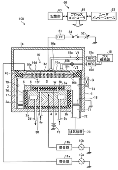
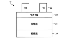
- A plasma processing method where an organic film, mask film, and resist film are sequentially treated with plasma, using reformed gases like H2 or hydrogen halide gases at low temperatures (-20°C or lower), to modify the resist film and improve its surface roughness and etching resistance, thereby maintaining processing accuracy.


Plasma enhanced processing, and related processing chambers, methods, and systems for semiconductor manufacturing
PatentWO2025159831A1
Innovation
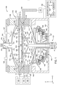
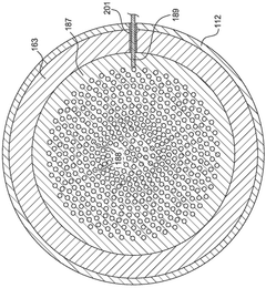
- A method involving plasma enhanced processing, where a plasma is ignited in a processing chamber, and a deposition precursor is flowed over a substrate at low pressures and controlled temperatures, with gas flows through the chamber's lid and sidewall, using inductive coils and RF coils to generate and control the plasma, ensuring uniform film growth and dopant concentration.
Environmental Impact and Sustainability
Plasma treatment in semiconductor manufacturing, while offering significant technological advantages, presents notable environmental challenges that the industry must address. The process consumes substantial energy, particularly in generating and maintaining plasma states, contributing to the semiconductor industry's carbon footprint. Modern fabrication facilities have implemented energy recovery systems and more efficient power supplies to mitigate this impact, reducing energy consumption by up to 30% compared to earlier generation equipment.
Chemical usage represents another environmental concern, as plasma processes often utilize greenhouse gases like perfluorocarbons (PFCs) and sulfur hexafluoride (SF6), which have global warming potentials thousands of times greater than CO2. Leading manufacturers have developed abatement systems that can neutralize over 95% of these emissions before release, significantly reducing their environmental impact. Additionally, closed-loop systems that recapture and purify process gases for reuse are becoming increasingly common in advanced facilities.
Water consumption remains a critical sustainability challenge, with semiconductor manufacturing requiring ultra-pure water for cleaning and processing. A typical fabrication plant may use 2-4 million gallons of water daily. Progressive manufacturers have implemented water recycling systems that can reclaim up to 85% of process water, substantially reducing freshwater requirements and wastewater discharge.
Waste management presents further challenges, as plasma etching processes generate hazardous byproducts requiring specialized disposal. The industry has developed advanced filtration and treatment technologies that can reduce hazardous waste volume by up to 60%. Some facilities have achieved zero-landfill status through comprehensive recycling programs and waste-to-energy conversion systems.
Looking forward, sustainable plasma treatment technologies are emerging as a priority research area. Low-temperature atmospheric plasma processes that operate without vacuum systems can reduce energy requirements by up to 40%. Alternative chemistries using less environmentally harmful gases are showing promising results in research settings, potentially eliminating the need for the most problematic greenhouse gases within the next decade.
The semiconductor industry has established collaborative initiatives like the Semiconductor Climate Consortium to accelerate sustainability improvements across the supply chain. These efforts align with increasing regulatory pressure and customer demands for environmentally responsible manufacturing practices, driving continuous innovation in greener plasma treatment technologies.
Cost-Benefit Analysis of Advanced Plasma Systems
The implementation of advanced plasma systems in semiconductor manufacturing represents a significant capital investment that must be carefully evaluated against potential returns. Initial acquisition costs for state-of-the-art plasma treatment equipment typically range from $2-5 million per unit, with additional expenses for facility modifications, specialized infrastructure, and safety systems that can add 15-30% to the base price.
Operating costs present another substantial consideration, including power consumption (plasma systems often require 50-200 kW continuous operation), specialized gases (which may cost $1,000-5,000 per month depending on process requirements), and maintenance contracts that generally run 8-12% of the initial equipment cost annually.
However, these investments deliver measurable financial benefits across multiple dimensions. Production yield improvements of 5-15% are commonly reported after implementing advanced plasma treatment systems, directly increasing revenue potential. For a medium-sized fabrication facility producing 50,000 wafers monthly, even a 5% yield improvement can translate to $2-4 million in additional monthly revenue.
Quality enhancement represents another significant benefit, with plasma-treated components showing 30-50% fewer defects and 20-40% improved reliability metrics. This reduction in failure rates substantially decreases warranty costs and customer returns, protecting both revenue and brand reputation.
Process efficiency gains are equally important, with modern plasma systems reducing cycle times by 15-25% compared to conventional methods. This throughput improvement effectively increases production capacity without requiring additional equipment or facility expansion, optimizing capital utilization.
The environmental cost-benefit equation also favors advanced plasma systems. While traditional wet chemical processes generate substantial hazardous waste requiring expensive disposal (often $10-20 per gallon), plasma treatments produce minimal waste streams. The resulting reduction in environmental compliance costs and potential liability exposure represents a significant though often undervalued financial benefit.
Return on investment calculations typically show advanced plasma systems reaching breakeven within 12-24 months of implementation, with subsequent years delivering substantial positive returns. This favorable financial profile explains the accelerating adoption of these technologies across the semiconductor manufacturing landscape despite their substantial upfront costs.
Unlock deeper insights with Patsnap Eureka Quick Research — get a full tech report to explore trends and direct your research. Try now!
Generate Your Research Report Instantly with AI Agent
Supercharge your innovation with Patsnap Eureka AI Agent Platform!