How To Advance Tungsten Sputtering Targets?
Tungsten Sputtering Evolution
Tungsten sputtering technology has undergone significant evolution since its inception in the mid-20th century. The journey began with simple DC sputtering systems, which were limited in their ability to deposit uniform and high-quality tungsten films. As the demand for more advanced electronic devices grew, so did the need for improved sputtering techniques.
The 1970s saw the introduction of magnetron sputtering, a breakthrough that dramatically enhanced the efficiency and quality of tungsten deposition. This technique utilized magnetic fields to confine electrons near the target surface, increasing ionization and sputtering rates. The result was denser films with better adhesion and uniformity, crucial for the emerging semiconductor industry.
In the 1980s and 1990s, further advancements came with the development of high-power impulse magnetron sputtering (HiPIMS). This technique applied short, high-power pulses to the sputtering target, creating a highly ionized plasma. HiPIMS allowed for even greater control over film properties, including density, stress, and microstructure, making it particularly valuable for tungsten coatings in cutting tools and wear-resistant applications.
The turn of the millennium brought about refinements in target design and cooling systems. Segmented targets and optimized cooling mechanisms addressed issues of target deformation and overheating, enabling longer sputtering runs and more consistent film quality. These improvements were crucial for large-area coatings and high-volume production environments.
Recent years have seen a focus on nanostructured tungsten films and multi-component systems. Advanced process control and in-situ monitoring techniques have enabled the deposition of tungsten films with precisely tailored properties at the nanoscale. This has opened up new applications in fields such as nuclear fusion research, where nanostructured tungsten coatings show promise for plasma-facing components.
The integration of computational modeling and artificial intelligence has further accelerated the evolution of tungsten sputtering. These tools allow for the prediction of optimal sputtering parameters and film properties, reducing development time and costs. Machine learning algorithms are now being employed to fine-tune processes in real-time, ensuring consistent quality across production runs.
Looking ahead, the evolution of tungsten sputtering targets is likely to continue in several directions. One promising area is the development of composite and alloy targets, which could enable the deposition of multi-functional coatings in a single process. Additionally, there is growing interest in environmentally friendly sputtering processes, with research focused on reducing energy consumption and minimizing waste materials.
Market Demand Analysis
The market demand for advanced tungsten sputtering targets has been steadily increasing, driven by the growing semiconductor and electronics industries. As these sectors continue to evolve, the need for high-performance sputtering targets becomes more critical. The global sputtering targets market is expected to expand significantly in the coming years, with tungsten targets playing a crucial role in this growth.
Tungsten sputtering targets are widely used in the production of thin films for various applications, including integrated circuits, flat panel displays, and solar cells. The semiconductor industry, in particular, relies heavily on tungsten targets for the deposition of interconnect layers and diffusion barriers. As chip manufacturers push for smaller and more efficient devices, the demand for higher-quality tungsten targets with improved uniformity and purity has intensified.
The electronics industry's shift towards miniaturization and increased functionality has further fueled the demand for advanced tungsten sputtering targets. These targets are essential in producing thin films with precise thickness control and excellent adhesion properties, which are crucial for the development of next-generation electronic devices.
In the solar energy sector, tungsten targets are used in the production of thin-film solar cells. As the world moves towards renewable energy sources, the demand for more efficient and cost-effective solar panels has led to increased research and development in thin-film technology, subsequently driving the need for advanced tungsten sputtering targets.
The automotive industry has also emerged as a significant consumer of tungsten sputtering targets. With the growing adoption of electric vehicles and advanced driver assistance systems, there is an increased demand for sensors and electronic components that rely on thin-film technology. This trend is expected to contribute to the overall market growth for tungsten targets.
Geographically, Asia-Pacific remains the largest market for tungsten sputtering targets, primarily due to the concentration of semiconductor and electronics manufacturing in countries like China, South Korea, and Taiwan. However, North America and Europe are also witnessing steady growth in demand, driven by advancements in medical devices, aerospace, and defense technologies.
The market demand for tungsten sputtering targets is not only focused on quantity but also on quality and performance. End-users are increasingly seeking targets with higher density, improved microstructure, and enhanced sputtering efficiency. This has led to a growing emphasis on research and development to create advanced tungsten targets that can meet these stringent requirements and support the development of cutting-edge technologies.
Current Challenges
Tungsten sputtering targets face several significant challenges in their current state of development and application. These challenges primarily stem from the inherent properties of tungsten and the demanding requirements of modern thin film deposition processes.
One of the primary challenges is the brittleness of tungsten, which makes it susceptible to cracking during the manufacturing process and subsequent use. This brittleness can lead to target failure, resulting in costly downtime and potential contamination of the sputtering chamber. The high melting point of tungsten, while advantageous for many applications, also presents difficulties in target fabrication and bonding to backing plates.
The density of tungsten poses another challenge, as it can lead to non-uniform erosion patterns during sputtering. This non-uniformity affects the consistency of the deposited films and can reduce target utilization efficiency. Additionally, the high atomic weight of tungsten can cause increased energy requirements for sputtering, potentially leading to higher operating costs and reduced throughput.
Impurity control remains a critical issue in tungsten sputtering targets. Even minute amounts of contaminants can significantly impact the performance of the deposited films, particularly in sensitive applications such as semiconductor manufacturing. Achieving and maintaining the required purity levels throughout the target lifecycle is an ongoing challenge for manufacturers and end-users alike.
The grain structure of tungsten targets also presents difficulties. Large grains or inconsistent grain sizes can lead to variations in sputtering rates and film properties across the target surface. This can result in thickness non-uniformities and compositional variations in the deposited films, which are particularly problematic in precision applications.
Another challenge lies in the optimization of target geometry and design. Traditional planar targets may not provide optimal material utilization or uniform erosion profiles. Developing advanced target shapes that improve sputtering efficiency while maintaining structural integrity is an area of ongoing research and development.
The thermal management of tungsten targets during high-power sputtering processes is also a significant concern. The high thermal conductivity of tungsten can lead to localized heating and potential target deformation or failure if not properly managed. Designing effective cooling systems that can handle the heat load without compromising target performance is a complex engineering challenge.
Lastly, the environmental and economic aspects of tungsten target production and recycling present ongoing challenges. The scarcity of tungsten as a resource and the energy-intensive processes involved in target manufacturing necessitate the development of more sustainable practices, including improved recycling techniques and the exploration of alternative materials or composites that can match or exceed the performance of pure tungsten targets.
Existing Solutions
01 Composition and structure of tungsten sputtering targets
Tungsten sputtering targets are developed with specific compositions and structures to enhance their performance. This includes controlling the grain size, density, and purity of the tungsten material. Advanced manufacturing techniques are employed to achieve desired microstructures and properties, such as improved uniformity and reduced defects.- Composition and structure of tungsten sputtering targets: Tungsten sputtering targets are designed with specific compositions and structures to enhance their performance. This includes controlling the grain size, density, and purity of the tungsten material. Advanced manufacturing techniques are employed to achieve desired microstructures and properties, which can significantly impact the quality of the deposited thin films.
- Doping and alloying of tungsten sputtering targets: Doping or alloying tungsten sputtering targets with other elements can improve their properties and performance. This may include adding elements like rhenium, molybdenum, or tantalum to enhance mechanical strength, thermal stability, or electrical conductivity. The precise control of dopant concentrations and distribution is crucial for achieving optimal target characteristics.
- Manufacturing processes for tungsten sputtering targets: Various manufacturing processes are employed to produce high-quality tungsten sputtering targets. These may include powder metallurgy techniques, hot isostatic pressing, electron beam melting, or additive manufacturing methods. Each process aims to achieve specific target properties such as uniformity, density, and microstructure, which are critical for consistent sputtering performance.
- Surface treatment and finishing of tungsten sputtering targets: Surface treatment and finishing techniques are applied to tungsten sputtering targets to enhance their performance and longevity. This may include polishing, etching, or coating processes to improve surface roughness, remove contaminants, and optimize sputtering characteristics. Proper surface preparation is essential for achieving high-quality thin film deposition.
- Recycling and reprocessing of tungsten sputtering targets: Recycling and reprocessing methods for used tungsten sputtering targets are developed to recover valuable materials and reduce waste. These processes may involve chemical or physical separation techniques to extract pure tungsten or other valuable components. Recycling not only reduces environmental impact but also helps in maintaining a sustainable supply chain for tungsten sputtering targets.
02 Doping and alloying of tungsten sputtering targets
Doping or alloying tungsten sputtering targets with other elements can improve their properties and performance. This may include adding elements like rhenium, molybdenum, or tantalum to enhance mechanical strength, thermal stability, or electrical conductivity. The precise control of dopant concentrations and distribution is crucial for optimizing target characteristics.Expand Specific Solutions03 Manufacturing processes for tungsten sputtering targets
Various manufacturing processes are employed to produce high-quality tungsten sputtering targets. These may include powder metallurgy techniques, hot isostatic pressing, electron beam melting, or additive manufacturing methods. The choice of manufacturing process significantly influences the target's microstructure, density, and overall performance in sputtering applications.Expand Specific Solutions04 Surface treatment and finishing of tungsten sputtering targets
Surface treatment and finishing techniques are applied to tungsten sputtering targets to enhance their performance and longevity. This may include polishing, etching, or coating processes to improve surface roughness, remove contaminants, and optimize sputtering characteristics. Proper surface preparation is essential for achieving consistent and high-quality thin film deposition.Expand Specific Solutions05 Recycling and reprocessing of tungsten sputtering targets
Methods for recycling and reprocessing used tungsten sputtering targets are developed to recover valuable materials and reduce waste. This involves techniques for separating tungsten from other materials, purifying the recovered tungsten, and remanufacturing new targets. Efficient recycling processes contribute to sustainability and cost-effectiveness in the sputtering target industry.Expand Specific Solutions
Key Industry Players
The advancement of tungsten sputtering targets is in a mature yet evolving phase, with a growing market driven by increasing demand in semiconductor and electronics industries. The technology's maturity is evident from the involvement of established players like Mitsubishi Materials Corp., ULVAC, Inc., and Toshiba Corp., who have extensive experience in materials science and sputtering technologies. However, the field remains competitive with companies like Konfoong Materials International Co., Ltd. and GRIKIN Advanced Material Co., Ltd. pushing for innovations in target purity, density, and microstructure. The market is characterized by a mix of large multinational corporations and specialized materials suppliers, indicating a complex ecosystem with opportunities for both technological breakthroughs and incremental improvements.
Mitsubishi Materials Corp.
ULVAC, Inc.
Core Innovations
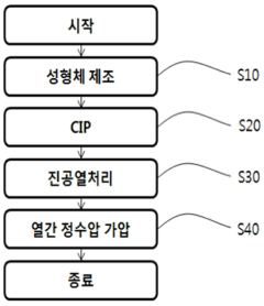
- A manufacturing method involving high-purity tungsten powder molding, cold isostatic pressing (CIP), vacuum heat treatment, and hot isostatic pressing is employed to produce a tungsten target with fine crystal grains and high density, minimizing impurity contamination and grain growth.
- A method involving hot press sintering and hot isostatic pressure sintering using tungsten powder with a large specific surface area, achieving a relative density of 99% and average grain size of 100 μm or less, reduces particle defects and production costs.
Material Characterization
Material characterization plays a crucial role in advancing tungsten sputtering targets. The analysis of the microstructure, composition, and properties of tungsten materials is essential for optimizing their performance in sputtering applications. Advanced characterization techniques provide valuable insights into the target's behavior during the sputtering process and help identify areas for improvement.
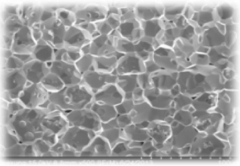
X-ray diffraction (XRD) is a fundamental technique used to determine the crystalline structure of tungsten targets. This method reveals information about grain size, texture, and phase composition, which directly influence the sputtering yield and film quality. Electron microscopy techniques, such as scanning electron microscopy (SEM) and transmission electron microscopy (TEM), offer high-resolution imaging of the target surface and internal structure. These methods are invaluable for examining grain boundaries, defects, and impurities that can affect target performance.
Chemical analysis techniques, including X-ray fluorescence (XRF) and inductively coupled plasma mass spectrometry (ICP-MS), are employed to determine the elemental composition and purity of tungsten targets. These methods can detect trace impurities that may impact the sputtered film's properties. Energy-dispersive X-ray spectroscopy (EDS) coupled with electron microscopy provides localized chemical information, allowing for the identification of compositional variations across the target.
Mechanical properties of tungsten targets are assessed through hardness testing, tensile strength measurements, and fracture toughness evaluations. These characteristics are critical for predicting target longevity and resistance to thermal stress during sputtering. Thermal analysis techniques, such as differential scanning calorimetry (DSC) and thermogravimetric analysis (TGA), provide insights into the target's behavior under varying temperature conditions, which is crucial for high-power sputtering applications.
Surface analysis techniques, including X-ray photoelectron spectroscopy (XPS) and Auger electron spectroscopy (AES), are employed to study the chemical state and composition of the target surface. This information is vital for understanding surface oxidation and contamination, which can significantly affect sputtering performance. Atomic force microscopy (AFM) and profilometry are used to characterize surface roughness and topography, factors that influence the uniformity of sputtered films.
Advanced characterization methods, such as electron backscatter diffraction (EBSD) and focused ion beam (FIB) microscopy, provide detailed information about grain orientation and three-dimensional microstructure. These techniques are particularly useful for studying the evolution of target microstructure during use and for developing strategies to enhance target longevity and performance.
By employing these diverse characterization techniques, researchers and manufacturers can gain a comprehensive understanding of tungsten sputtering targets. This knowledge forms the foundation for developing advanced manufacturing processes, optimizing target composition, and designing novel microstructures that enhance sputtering efficiency and film quality.
Environmental Considerations
The environmental considerations surrounding tungsten sputtering targets are becoming increasingly important as industries strive for more sustainable manufacturing processes. Tungsten, while a valuable material for sputtering applications, presents several environmental challenges throughout its lifecycle. The extraction and processing of tungsten ore can lead to significant land disturbance and habitat destruction. Moreover, the energy-intensive nature of tungsten production contributes to greenhouse gas emissions and climate change concerns.
In the manufacturing of sputtering targets, the use of chemical processes and high-temperature treatments can result in the release of potentially harmful substances into the environment. These may include volatile organic compounds (VOCs) and particulate matter, which can impact air quality and pose health risks to workers and surrounding communities. Additionally, the disposal of spent tungsten targets and associated waste materials requires careful management to prevent soil and water contamination.
To address these environmental issues, several strategies are being explored and implemented. One approach involves optimizing the sputtering process to increase target utilization efficiency, thereby reducing waste and the frequency of target replacements. This can be achieved through advanced target designs and improved process control systems. Furthermore, recycling and reclamation of spent tungsten targets are gaining traction as viable methods to minimize environmental impact and conserve resources.
Research into alternative materials and composite targets that can partially replace or reduce the amount of tungsten used is another avenue being pursued. These efforts aim to decrease the reliance on tungsten extraction while maintaining or improving the performance of sputtering applications. Additionally, the development of more environmentally friendly processing techniques, such as green chemistry approaches and closed-loop manufacturing systems, is underway to minimize the ecological footprint of tungsten target production.
The industry is also focusing on improving energy efficiency in the sputtering process itself. This includes the development of more efficient power supplies, cooling systems, and process optimization to reduce overall energy consumption. Such advancements not only contribute to environmental sustainability but also offer potential cost savings for manufacturers.
Regulatory compliance and voluntary environmental standards are driving further improvements in the environmental performance of tungsten sputtering target production and use. Companies are increasingly adopting life cycle assessment methodologies to evaluate and mitigate the environmental impacts across the entire value chain of tungsten targets. This holistic approach enables more informed decision-making and supports the development of more sustainable practices in the industry.