What are the Key Parameters Affecting Gallium Nitride Transistor Performance
OCT 14, 202510 MIN READ
Generate Your Research Report Instantly with AI Agent
Patsnap Eureka helps you evaluate technical feasibility & market potential.
GaN Transistor Evolution and Performance Objectives
Gallium Nitride (GaN) transistor technology has undergone significant evolution since its inception in the early 1990s. Initially developed for optoelectronic applications, GaN has emerged as a revolutionary wide bandgap semiconductor material that offers superior performance characteristics compared to traditional silicon-based technologies. The evolution of GaN transistors can be traced through several key developmental phases, each marked by significant technological breakthroughs and performance enhancements.
The first commercial GaN transistors appeared in the early 2000s, primarily targeting RF applications in telecommunications and defense sectors. These early devices demonstrated the fundamental advantages of GaN technology, including higher breakdown voltage and power density compared to silicon and gallium arsenide alternatives. However, they suffered from reliability issues, limited frequency response, and high production costs that restricted widespread adoption.
By the mid-2000s, significant progress was made in epitaxial growth techniques and device fabrication processes, leading to improved crystal quality and reduced defect densities. This period saw the emergence of GaN-on-SiC (Silicon Carbide) technology, which offered enhanced thermal management capabilities critical for high-power applications. The introduction of field plates and advanced passivation techniques during this phase helped mitigate electron trapping effects and improve reliability.
The 2010s marked a pivotal era with the commercialization of GaN-on-Si technology, dramatically reducing production costs while maintaining acceptable performance metrics. This development expanded GaN's application scope beyond RF into power electronics, including power supplies, motor drives, and automotive systems. During this period, enhancement-mode GaN transistors also gained traction, eliminating the need for negative gate bias and simplifying circuit design.
Current technological objectives for GaN transistors focus on several critical performance parameters. Increasing the maximum operating frequency beyond 100 GHz is essential for next-generation communication systems, particularly for 5G and future 6G applications. Simultaneously, improving power efficiency to exceed 80% at these frequencies remains a significant challenge that requires innovations in device architecture and materials.
Enhancing reliability under extreme operating conditions represents another crucial objective, particularly for automotive and aerospace applications where devices must function reliably at junction temperatures exceeding 200°C for thousands of hours. Researchers are also pursuing increased power density targets of 40-50 W/mm, which would enable unprecedented miniaturization of power systems.
The roadmap for GaN transistor evolution aims to achieve monolithic integration with control and protection circuitry, creating true "GaN-on-anything" capabilities that would revolutionize system design approaches. Additionally, reducing the cost per watt to levels competitive with silicon-based solutions remains a fundamental objective to drive widespread market adoption across consumer electronics and industrial applications.
Market Demand Analysis for GaN Power Electronics
The global market for GaN power electronics is experiencing unprecedented growth, driven by the increasing demand for high-performance, energy-efficient power devices across multiple industries. Current market valuations place the GaN power device sector at approximately 1.4 billion USD in 2023, with projections indicating a compound annual growth rate (CAGR) of 25-30% through 2030, potentially reaching 8.5 billion USD by the end of the decade.
This remarkable growth trajectory is primarily fueled by several key market drivers. The automotive sector represents the largest and fastest-growing segment, with electric vehicle manufacturers seeking more efficient power conversion solutions to extend range and reduce charging times. GaN transistors, with their superior switching speeds and lower on-resistance compared to silicon alternatives, enable more compact and efficient onboard chargers and DC-DC converters, addressing critical consumer concerns regarding EV adoption.
Consumer electronics constitutes another significant market segment, with manufacturers increasingly incorporating GaN-based fast chargers for smartphones, laptops, and other portable devices. The ability to deliver higher power in significantly smaller form factors has created a distinct competitive advantage for brands utilizing this technology, evidenced by the rapid proliferation of GaN chargers in premium device ecosystems.
Industrial applications represent a growing market opportunity, particularly in factory automation, renewable energy systems, and data centers. The superior thermal performance and reliability of GaN transistors in high-power applications make them increasingly attractive for industrial power supplies and motor drives, where efficiency improvements directly translate to operational cost savings.
Market research indicates regional variations in adoption rates, with Asia-Pacific currently leading GaN power electronics implementation, followed by North America and Europe. China, Japan, and South Korea have established strong manufacturing capabilities and domestic markets for GaN devices, while North American companies lead in innovation and intellectual property development.
Customer demand patterns reveal a growing preference for integrated GaN solutions rather than discrete components, with system-level benefits driving adoption decisions. Price sensitivity remains a significant factor limiting broader market penetration, as GaN solutions typically command a 30-50% premium over silicon alternatives, though this gap is narrowing as production volumes increase.
The competitive landscape is evolving rapidly, with traditional power semiconductor manufacturers expanding their GaN portfolios while specialized GaN-focused startups secure significant investment funding. This market dynamism is expected to accelerate technology development while driving down costs, further expanding addressable markets for GaN power electronics.
Current GaN Transistor Technology Challenges
Despite significant advancements in GaN transistor technology, several critical challenges continue to impede optimal performance and widespread adoption. The primary challenge remains thermal management, as GaN devices generate substantial heat during high-power operation. Current thermal dissipation techniques struggle to efficiently remove heat from the active region, leading to performance degradation and reliability concerns. Junction temperatures can exceed 250°C under high-power conditions, necessitating advanced cooling solutions beyond traditional methods.
Surface-related challenges present another significant hurdle. GaN transistors suffer from high densities of surface states and traps that cause current collapse, dynamic ON-resistance increase, and threshold voltage instability. These surface phenomena result in unpredictable device behavior during switching operations and compromise long-term reliability. Current passivation techniques provide only partial mitigation of these effects.
Buffer layer quality remains problematic, particularly when GaN is grown on non-native substrates like silicon or silicon carbide. The lattice mismatch introduces dislocations and defects that serve as leakage paths and trapping centers, degrading breakdown voltage and increasing dynamic losses. Typical dislocation densities in commercial GaN-on-Si devices range from 10^8 to 10^9 cm^-2, significantly higher than ideal.
Gate reliability issues persist across various GaN transistor architectures. In high-electron-mobility transistors (HEMTs), gate leakage currents increase under high electric fields, while in metal-insulator-semiconductor (MIS) structures, the gate dielectric quality and interface states remain challenging to control. These issues limit the maximum operating voltage and switching frequency capabilities.
Manufacturing scalability presents both technical and economic challenges. Current GaN wafer sizes lag behind silicon technology, with most production limited to 6-inch or 8-inch wafers. Additionally, process variations across wafers lead to inconsistent device performance, complicating large-scale production and increasing costs. The cost differential between GaN and silicon devices remains a significant barrier to widespread adoption in price-sensitive applications.
Packaging technology has not kept pace with GaN's inherent capabilities. Conventional packaging introduces parasitic inductances and capacitances that limit high-frequency performance. While advanced packaging solutions like embedded die technology show promise, they add complexity and cost to the manufacturing process.
Finally, standardization and qualification frameworks for GaN transistors remain underdeveloped compared to silicon technologies. The lack of universally accepted reliability testing protocols and qualification standards creates uncertainty for system designers and slows adoption in critical applications like automotive and aerospace.
Current Parameter Optimization Approaches
01 High-frequency performance enhancement in GaN transistors
Gallium Nitride (GaN) transistors demonstrate superior high-frequency performance due to their wide bandgap properties. Various structural modifications and fabrication techniques can enhance their frequency response, making them suitable for RF and microwave applications. These enhancements include optimized gate designs, reduced parasitic capacitances, and improved electron mobility in the two-dimensional electron gas (2DEG) channel, resulting in higher cutoff frequencies and improved power gain at high frequencies.- High-frequency performance enhancement techniques: Various techniques can be employed to enhance the high-frequency performance of Gallium Nitride (GaN) transistors. These include optimizing gate structures, reducing parasitic capacitances, and implementing advanced epitaxial layer designs. By carefully engineering these aspects, GaN transistors can achieve superior switching speeds and higher operating frequencies, making them suitable for RF and microwave applications. These enhancements enable improved power gain and efficiency at high frequencies compared to conventional semiconductor materials.
- Thermal management solutions for GaN transistors: Effective thermal management is crucial for maintaining the performance of GaN transistors under high-power operation. Various approaches include integrating heat dissipation structures, using thermally conductive substrates, and implementing novel packaging techniques. These solutions help to reduce thermal resistance and prevent performance degradation due to self-heating effects. Improved thermal management allows GaN transistors to operate reliably at higher power densities and maintains their electrical characteristics over extended operating periods.
- Substrate engineering for improved GaN transistor performance: The choice and engineering of substrate materials significantly impact GaN transistor performance. Techniques such as using silicon carbide substrates, engineered buffer layers, and strain management approaches can reduce defect densities and improve crystal quality. These advancements lead to enhanced electron mobility, reduced leakage currents, and improved breakdown voltage characteristics. Substrate engineering also enables better lattice matching, which is essential for high-quality epitaxial growth of GaN layers.
- Novel device structures for enhanced power handling: Innovative GaN transistor architectures have been developed to enhance power handling capabilities. These include vertical device structures, field-plate designs, and heterojunction configurations that optimize the distribution of electric fields. Such structures enable higher breakdown voltages, improved current handling, and reduced on-resistance. These advancements make GaN transistors particularly suitable for high-power switching applications in power electronics, where efficiency and power density are critical performance metrics.
- Surface passivation and interface control techniques: Surface passivation and interface control are essential for optimizing GaN transistor performance. Various dielectric materials and deposition techniques are employed to reduce surface states, trap densities, and current collapse phenomena. These approaches minimize dynamic on-resistance and improve reliability under switching conditions. Effective passivation also enhances long-term stability by protecting the device surface from environmental factors that could degrade performance over time.
02 Thermal management and reliability improvements
Thermal management is critical for GaN transistor performance and reliability. Advanced substrate materials, heat dissipation structures, and packaging techniques help manage the high power density of GaN devices. Innovations in this area include diamond heat spreaders, flip-chip bonding, and optimized device layouts that minimize thermal resistance. These improvements allow GaN transistors to operate reliably at higher power levels without performance degradation or premature failure due to thermal stress.Expand Specific Solutions03 Power handling capability enhancements
GaN transistors offer exceptional power handling capabilities due to their high breakdown voltage and current density. Techniques to further enhance power performance include field plate structures, buffer layer optimization, and advanced epitaxial growth methods. These improvements allow for higher operating voltages, reduced on-resistance, and better current handling, making GaN transistors ideal for power conversion applications where efficiency and power density are critical requirements.Expand Specific Solutions04 Novel device structures and fabrication methods
Innovative device architectures and fabrication techniques have been developed to enhance GaN transistor performance. These include vertical device structures, recessed gate designs, and novel barrier layers. Advanced epitaxial growth methods, such as metal-organic chemical vapor deposition (MOCVD) and molecular beam epitaxy (MBE), enable precise control of material quality and interfaces. These innovations result in improved carrier transport properties, reduced defect densities, and enhanced overall device performance.Expand Specific Solutions05 Integration and packaging solutions
Integration and packaging solutions play a crucial role in maximizing GaN transistor performance in practical applications. Advanced packaging techniques, such as system-in-package (SiP) and heterogeneous integration with silicon-based control circuits, enable compact and efficient power systems. Innovations in this area include low-inductance packaging, integrated passive components, and optimized thermal interfaces. These solutions help realize the full potential of GaN transistors in commercial applications by addressing system-level challenges.Expand Specific Solutions
Leading GaN Semiconductor Manufacturers and Competitors
The gallium nitride (GaN) transistor market is experiencing rapid growth, currently in the early mainstream adoption phase with increasing commercial applications. The market is projected to reach $2-3 billion by 2025, driven by demand in power electronics, RF applications, and electric vehicles. Key performance parameters include breakdown voltage, on-resistance, switching speed, and thermal management. Leading players like Wolfspeed, Texas Instruments, and Intel are advancing the technology through innovations in substrate materials, device structures, and packaging techniques. Asian manufacturers including TSMC, Sumitomo Electric, and Huawei are gaining market share through cost-effective manufacturing processes. Research institutions such as CEA and universities collaborate with industry to overcome challenges in reliability, cost reduction, and integration with conventional silicon-based electronics.
MACOM Technology Solutions Holdings, Inc.
Technical Solution: MACOM has developed a unique GaN-on-Silicon technology platform that addresses key performance parameters through innovative epitaxial growth techniques. Their approach focuses on managing the lattice mismatch between GaN and silicon substrates (approximately 17%) through proprietary strain management layers and AlN nucleation layers with precisely controlled thickness (typically 100-200nm). MACOM's GaN transistors feature optimized AlGaN barrier layers with aluminum content carefully tuned between 15-30% to balance 2DEG density and mobility. Their devices incorporate advanced gate structures with gate-to-channel distances optimized to less than 20nm, enabling high transconductance (>300 mS/mm) while maintaining good pinch-off characteristics. MACOM has also developed specialized surface passivation techniques using multi-layer dielectric stacks to minimize surface traps and RF dispersion effects, resulting in improved linearity and power-added efficiency (PAE) exceeding 60% at X-band frequencies.
Strengths: Cost-effective GaN-on-Silicon approach enables broader market adoption; strong RF design expertise; established manufacturing partnerships for volume production. Weaknesses: Lower thermal conductivity of silicon substrates compared to SiC limits power handling; higher defect densities can impact reliability in extreme environments; challenges in very high frequency applications (>20GHz).
Wolfspeed, Inc.
Technical Solution: Wolfspeed has pioneered silicon carbide and GaN solutions for over 35 years, developing advanced GaN-on-SiC HEMT (High Electron Mobility Transistor) technology. Their GaN transistors feature optimized epitaxial layer structures with precise control of aluminum content in the AlGaN barrier layer (typically 20-30%) to optimize 2DEG (Two-Dimensional Electron Gas) formation. They've implemented field plates and gate engineering techniques to increase breakdown voltage while maintaining high current density (>1A/mm). Wolfspeed's GaN transistors demonstrate exceptional power density (>5W/mm) and achieve frequencies up to 100GHz with optimized gate length (<0.25μm). Their proprietary surface passivation techniques effectively mitigate current collapse and dispersion effects, resulting in more stable device performance under various operating conditions.
Strengths: Industry-leading power density and frequency performance; extensive experience in wide bandgap semiconductors; vertical integration from substrate to device manufacturing. Weaknesses: Higher cost compared to silicon-based alternatives; thermal management challenges at extreme power densities; reliability concerns in certain high-stress applications.
Critical Patents and Research in GaN Transistor Design
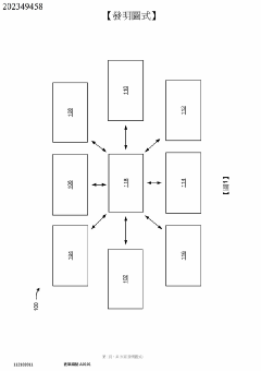
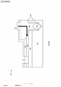
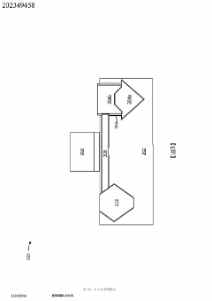
Semiconductor device
PatentPendingTW202349458A
Innovation
- Using gallium nitride and carbon (GaN:C) composite layers as a buffer between GaN drain and silicon substrate to reduce lattice mismatch defects and improve electrical performance.
- Implementing GaN:C buffer layers to reduce current leakage into the substrate, thereby improving the electrical performance of the transistor.
- Silicon implantation in aluminum nitride liner for GaN drain to reduce contact resistance at the GaN-Si interface.

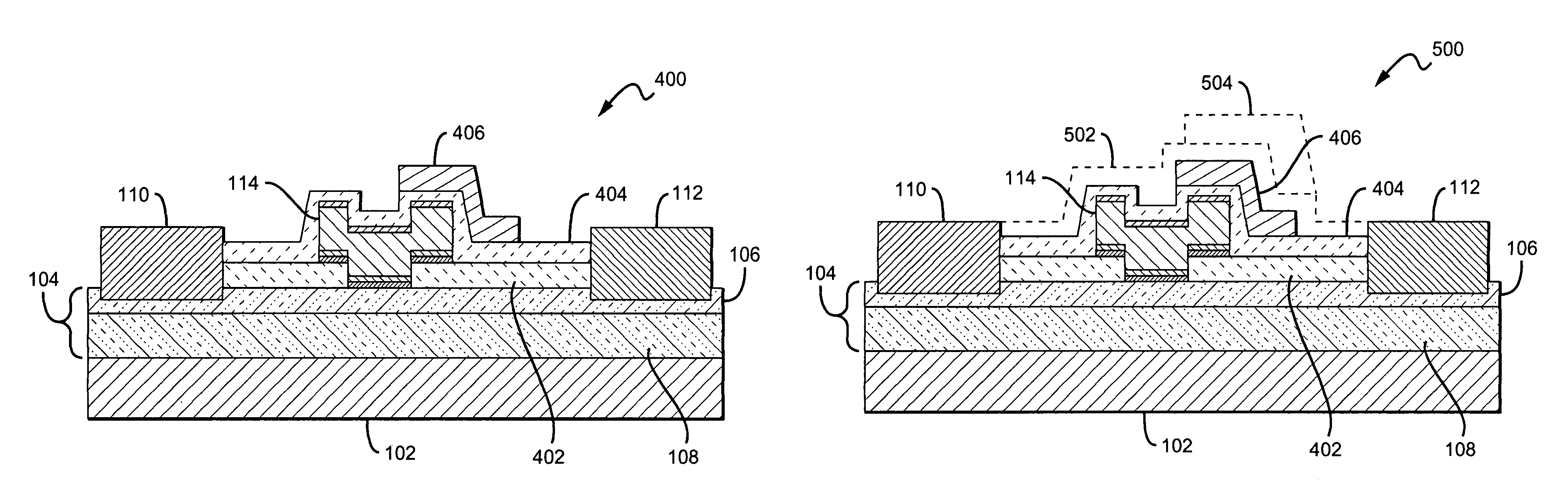
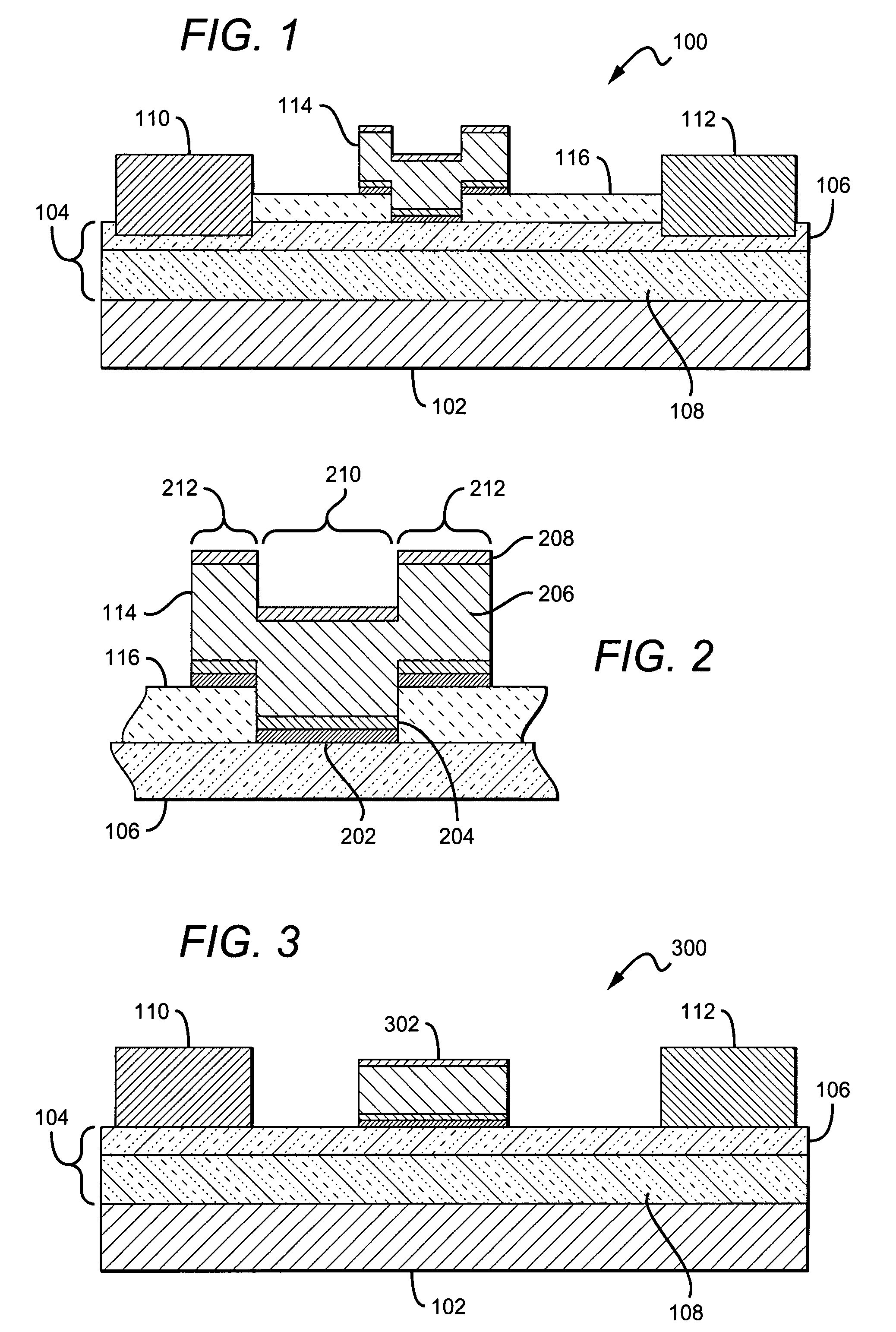
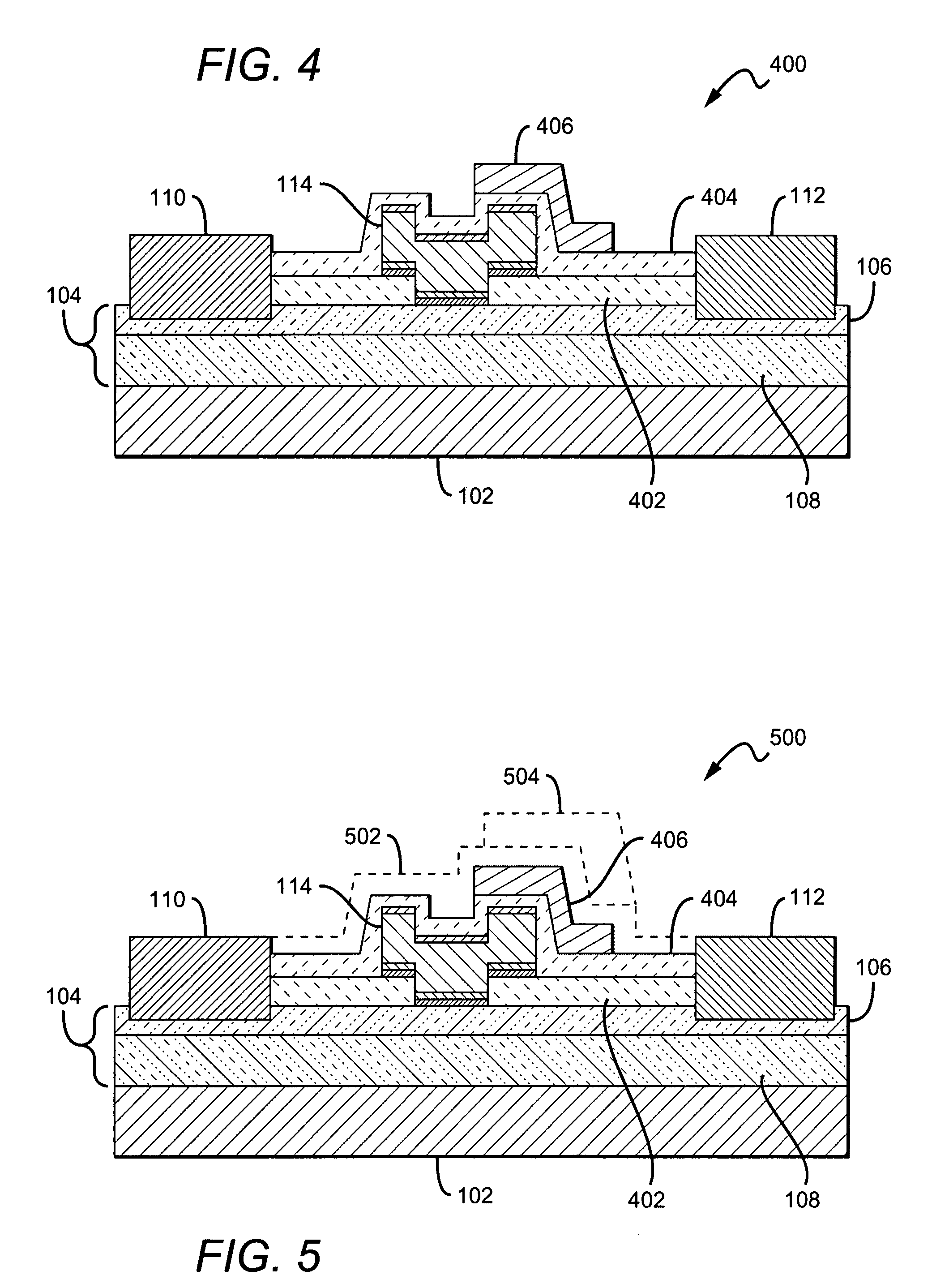
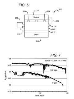
High temperature performance capable gallium nitride transistor
PatentActiveUS8212290B2
Innovation
- The use of a gate electrode made from materials with a high Schottky barrier, such as platinum (Pt), tungsten (W), molybdenum (Mo), chromium (Cr), or nickel-chromium alloys (NiCr), and the incorporation of spacer layers and field plates to reduce peak electric fields and enhance reliability, while maintaining low degradation at high temperatures.
Thermal Management Solutions for GaN Devices
Thermal management represents a critical challenge in the development and application of Gallium Nitride (GaN) transistors. As GaN devices operate at higher power densities and frequencies than traditional silicon-based semiconductors, they generate significant heat that must be efficiently dissipated to maintain optimal performance and reliability.
Current thermal management solutions for GaN devices can be categorized into several approaches. Advanced packaging techniques utilize materials with superior thermal conductivity such as copper-tungsten composites and diamond-based substrates. These materials facilitate more efficient heat transfer from the active device region to the external environment, reducing thermal resistance by up to 30% compared to conventional packaging.
Integrated heat spreaders represent another effective solution, where thermally conductive materials are directly incorporated into the device structure. Silicon carbide (SiC) substrates have emerged as a preferred option due to their thermal conductivity of approximately 490 W/mK, significantly outperforming silicon's 150 W/mK. This integration allows heat to dissipate laterally before reaching thermal bottlenecks in the vertical direction.
Active cooling systems, including microfluidic channels and two-phase cooling technologies, have demonstrated remarkable thermal management capabilities for high-power GaN applications. Recent research has shown that microfluidic cooling can reduce junction temperatures by up to 40°C under high-power operation conditions, extending device lifetime and maintaining performance parameters.
Thermal simulation and modeling tools have become essential in optimizing GaN device designs before fabrication. Finite element analysis (FEA) and computational fluid dynamics (CFD) enable accurate prediction of thermal hotspots and optimization of heat dissipation pathways. These computational approaches have reduced design iteration cycles by approximately 40% while improving thermal performance.
Novel materials research continues to advance thermal management capabilities. Graphene-based thermal interface materials have demonstrated thermal conductivity exceeding 2000 W/mK in laboratory settings, potentially revolutionizing heat transfer in next-generation GaN devices. Additionally, phase-change materials incorporated into packaging solutions provide temperature stabilization during transient operation conditions.
System-level thermal management approaches consider the entire application environment, incorporating optimized heat sinks, forced-air cooling, and strategic device placement to maximize thermal performance. These holistic solutions have proven particularly effective in telecommunications infrastructure and automotive applications where environmental conditions vary significantly.
The continued advancement of these thermal management solutions will be crucial for enabling GaN transistors to reach their full performance potential across expanding application domains, from power electronics to RF communications and beyond.
Reliability and Lifetime Assessment Methodologies
Reliability and lifetime assessment of Gallium Nitride (GaN) transistors requires sophisticated methodologies to accurately predict performance degradation under various operational conditions. The industry has developed several standardized approaches to evaluate GaN device reliability, with accelerated life testing being the cornerstone methodology. This technique subjects devices to elevated stress conditions—including higher temperatures, voltages, and current densities—to induce failure mechanisms that would normally occur over much longer timeframes under normal operating conditions.
Time-dependent dielectric breakdown (TDDB) testing has emerged as a critical assessment method specifically tailored for GaN high-electron-mobility transistors (HEMTs). This methodology evaluates the gate dielectric integrity by applying constant voltage stress while monitoring leakage current until catastrophic failure occurs. The resulting data enables the extraction of lifetime models based on voltage acceleration factors and activation energies.
Hot carrier injection (HCI) testing represents another vital methodology for GaN reliability assessment. This approach evaluates degradation caused by high-energy carriers damaging the semiconductor-dielectric interface or becoming trapped in the dielectric layer. For GaN devices, HCI testing typically involves operating the transistor at high drain-source voltages while monitoring shifts in threshold voltage and transconductance.
Statistical analysis frameworks have been developed to interpret reliability data from these methodologies. The Weibull distribution has proven particularly effective for modeling GaN device failures, allowing engineers to extrapolate failure rates at normal operating conditions from accelerated test data. Mean Time To Failure (MTTF) and Failure In Time (FIT) metrics derived from these distributions provide quantitative reliability benchmarks for comparing different device technologies and manufacturing processes.
Non-destructive reliability monitoring techniques have gained prominence in recent years. These include low-frequency noise measurements, which can detect early indicators of degradation before device parameters show measurable shifts. Similarly, pulsed I-V characterization allows for the evaluation of trapping effects without causing permanent device degradation, providing insights into potential reliability issues.
Mission profile-based lifetime assessment has emerged as an advanced methodology that considers actual application conditions rather than constant stress scenarios. This approach combines device-level reliability models with system-level operational profiles to predict lifetime in specific applications. For power electronics applications using GaN transistors, thermal cycling, power cycling, and environmental stress screening have become standard components of comprehensive reliability assessment protocols.
Unlock deeper insights with Patsnap Eureka Quick Research — get a full tech report to explore trends and direct your research. Try now!
Generate Your Research Report Instantly with AI Agent
Supercharge your innovation with Patsnap Eureka AI Agent Platform!