

P–N Junction vs Zener Diode: Breakdown Behavior
SEP 5, 20259 MIN READ
Generate Your Research Report Instantly with AI Agent
Patsnap Eureka helps you evaluate technical feasibility & market potential.
Semiconductor Junction Breakdown Evolution and Objectives
The evolution of semiconductor junction breakdown mechanisms represents a fundamental area of study in solid-state physics and electronic device engineering. Since the discovery of the p-n junction in the early 1940s, researchers have progressively refined their understanding of breakdown phenomena, which occur when electric fields across semiconductor junctions exceed critical thresholds.
The initial theoretical framework for junction breakdown was established by Carl Wagner and William Shockley in the late 1940s, followed by significant contributions from K.G. McKay and K.B. McAfee in the early 1950s. Their work differentiated between two primary breakdown mechanisms: avalanche multiplication and quantum tunneling (Zener effect), which continue to form the cornerstone of modern semiconductor device physics.
The technological trajectory has evolved from simple germanium diodes with poorly controlled breakdown characteristics to precisely engineered silicon and compound semiconductor devices with predictable and exploitable breakdown behaviors. This evolution has enabled the development of voltage reference circuits, protection devices, and specialized components like Zener diodes, transient voltage suppressors, and avalanche photodiodes.
Current research objectives focus on understanding breakdown behavior at nanoscale dimensions, where quantum effects become increasingly prominent. As device geometries continue to shrink below 10nm, conventional breakdown models require significant refinement to account for quantum confinement effects and ballistic transport phenomena.
Another critical objective involves characterizing breakdown mechanisms in wide-bandgap semiconductors such as silicon carbide (SiC) and gallium nitride (GaN). These materials offer substantially higher breakdown fields (>3 MV/cm) compared to silicon (0.3 MV/cm), enabling power devices with superior performance in high-voltage applications.
Temperature dependence represents another key research focus, particularly understanding how breakdown voltage varies across extreme temperature ranges (-55°C to +300°C) in modern automotive and industrial applications. This knowledge is essential for designing robust protection circuits and reliable power systems.
The ultimate goal of current research is to develop comprehensive predictive models that accurately describe breakdown phenomena across diverse semiconductor materials, device geometries, and operating conditions. These models must bridge quantum mechanical effects at the nanoscale with macroscopic device behavior to enable next-generation semiconductor technologies with optimized performance, reliability, and energy efficiency.
Market Applications and Demand for Breakdown Devices
The breakdown behavior of semiconductor devices has created a substantial market across multiple industries, with both P-N junctions and Zener diodes serving critical functions in various applications. The global voltage regulator market, where Zener diodes play a prominent role, was valued at approximately 1.6 billion USD in 2021 and is projected to grow at a CAGR of 5.8% through 2028, driven by increasing demand for stable power supplies in electronic devices.
Power electronics represents the largest application segment for breakdown devices, accounting for nearly 40% of the market share. The controlled breakdown behavior of Zener diodes makes them essential components in voltage regulation circuits, surge protection systems, and reference voltage generators. These applications are particularly vital in consumer electronics, which has seen exponential growth with the proliferation of smartphones, laptops, and IoT devices.
The automotive industry has emerged as a rapidly expanding market for breakdown devices, particularly with the transition toward electric vehicles (EVs). Modern vehicles contain an average of 2,000-3,000 semiconductor components, with voltage regulation and protection circuits being critical for battery management systems, motor controllers, and advanced driver-assistance systems. The EV market's compound annual growth rate of approximately 24% is directly driving demand for high-reliability breakdown devices that can operate under extreme temperature conditions.
Telecommunications infrastructure represents another significant market segment, where the avalanche breakdown characteristics of specially designed P-N junctions are utilized in high-frequency applications. The ongoing global 5G network deployment has intensified demand for robust semiconductor components that can handle increased power densities and frequencies.
Industrial automation and control systems rely heavily on precision voltage reference circuits where Zener diodes' predictable breakdown behavior provides stable reference points. This sector is expected to grow substantially as Industry 4.0 initiatives accelerate worldwide, with particular emphasis on energy-efficient manufacturing processes that require precise power management.
Renewable energy systems constitute an emerging application area with significant growth potential. Solar inverters and wind power converters require robust protection against voltage fluctuations, creating demand for specialized breakdown devices that can operate reliably under variable environmental conditions. The renewable energy sector's projected growth of 8-10% annually through 2030 will further expand this market segment.
Medical devices represent a premium niche market where ultra-reliable breakdown devices command higher margins due to stringent regulatory requirements. Applications include patient monitoring equipment, diagnostic tools, and implantable devices where stable voltage references are critical for accurate measurements and patient safety.
Current P-N and Zener Diode Breakdown Mechanisms
The breakdown behavior in semiconductor devices represents a critical operational characteristic that determines their functionality in electronic circuits. In P-N junctions, two primary breakdown mechanisms exist: avalanche breakdown and Zener breakdown. These mechanisms, while fundamentally different in their physical processes, both result in a rapid increase in current flow when a reverse bias exceeds a critical threshold.
Avalanche breakdown occurs when the electric field across the depletion region becomes sufficiently strong to accelerate free electrons to velocities capable of impact ionization. This process creates electron-hole pairs through collision with lattice atoms, which in turn generate additional carriers in a multiplicative effect. The phenomenon typically manifests in junctions with wider depletion regions and at higher reverse voltages, generally above 6-8V.
Zener breakdown, conversely, operates through quantum mechanical tunneling. When the electric field intensity reaches approximately 3×10^7 V/m, the energy bands bend significantly, allowing valence electrons to tunnel directly into the conduction band without gaining sufficient energy for impact ionization. This mechanism predominates in heavily doped junctions with narrower depletion regions and occurs at lower reverse voltages, typically below 5-6V.
Zener diodes are specifically engineered to exploit these breakdown mechanisms for voltage regulation applications. Their construction involves precise doping concentrations to control the breakdown voltage with high accuracy. Modern manufacturing techniques can produce Zener diodes with breakdown voltages ranging from 1.8V to hundreds of volts, with tolerances as tight as ±1%.
Temperature dependence represents another crucial distinction between these mechanisms. Zener breakdown exhibits a negative temperature coefficient (breakdown voltage decreases with increasing temperature), while avalanche breakdown demonstrates a positive temperature coefficient. Interestingly, commercial Zener diodes operating around 5-6V often display near-zero temperature coefficients due to the competing effects of both mechanisms occurring simultaneously.
Recent advancements in semiconductor fabrication have enabled enhanced control over breakdown characteristics. Techniques such as ion implantation allow for precise doping profiles, while epitaxial growth methods produce more uniform junction interfaces. These improvements have led to Zener diodes with sharper knee characteristics, lower noise, and improved long-term stability.
The current understanding of breakdown mechanisms has been significantly enhanced through advanced characterization techniques. High-resolution transmission electron microscopy (HRTEM) and scanning capacitance microscopy (SCM) have provided direct visualization of depletion regions and doping profiles. Additionally, numerical simulation tools incorporating quantum mechanical models now accurately predict breakdown behavior across a wide range of operating conditions.
Comparative Analysis of P-N and Zener Breakdown Solutions
01 Zener diode breakdown mechanisms
Zener diodes operate based on specific breakdown mechanisms that occur at the P-N junction. When reverse biased beyond a certain voltage threshold, these diodes exhibit controlled breakdown behavior. This breakdown can occur through two primary mechanisms: Zener breakdown (quantum mechanical tunneling) at lower voltages and avalanche breakdown at higher voltages. The design of the junction doping profiles and semiconductor materials determines the predominant breakdown mechanism and the resulting electrical characteristics.- Zener diode breakdown mechanisms: Zener diodes operate based on specific breakdown mechanisms that occur at the P-N junction. When reverse biased beyond a certain voltage threshold, these diodes exhibit controlled breakdown behavior. This breakdown can occur through two primary mechanisms: Zener breakdown (quantum tunneling) at lower voltages and avalanche breakdown at higher voltages. The design of the junction doping profiles and semiconductor materials determines the predominant breakdown mechanism and the resulting electrical characteristics.
- P-N junction design for controlled breakdown: The design of P-N junctions significantly influences the breakdown behavior of Zener diodes. Factors such as doping concentration, junction depth, and geometric configuration affect the breakdown voltage and stability. Specialized junction designs can create precise breakdown voltages and sharp knee characteristics. Advanced manufacturing techniques allow for tailored junction profiles that optimize breakdown behavior for specific applications while maintaining reliability under various operating conditions.
- Temperature effects on breakdown behavior: Temperature significantly impacts the breakdown behavior of P-N junctions in Zener diodes. As temperature increases, the breakdown voltage typically changes, with different coefficients depending on whether Zener or avalanche breakdown is dominant. Devices designed for voltage reference applications incorporate special structures to minimize temperature sensitivity. Some designs combine complementary temperature coefficients to achieve temperature-stable breakdown characteristics across wide operating temperature ranges.
- Advanced semiconductor materials for breakdown optimization: The choice of semiconductor materials plays a crucial role in determining the breakdown characteristics of P-N junctions. Beyond traditional silicon, materials such as silicon carbide, gallium nitride, and various compound semiconductors offer enhanced breakdown properties. These advanced materials enable higher breakdown voltages, better thermal performance, and improved reliability. Specialized doping profiles and material combinations can be engineered to achieve precise breakdown voltages and superior electrical performance.
- Fabrication techniques for controlled breakdown voltage: Specialized fabrication techniques are employed to achieve precise control over the breakdown behavior of P-N junctions in Zener diodes. These include ion implantation, epitaxial growth, and thermal diffusion processes that create specific doping profiles. The manufacturing methods directly influence the breakdown voltage, sharpness of the knee characteristic, and long-term stability. Advanced processing techniques allow for tight statistical control of breakdown parameters across production batches, ensuring consistency in device performance.
02 P-N junction design for controlled breakdown
The design of P-N junctions significantly influences the breakdown behavior of Zener diodes. By carefully controlling doping concentrations, junction depths, and geometric configurations, manufacturers can achieve precise breakdown voltages and sharp knee characteristics. Advanced junction designs incorporate specialized structures such as guard rings, field plates, or stepped junctions to prevent premature edge breakdown and ensure uniform current distribution across the device during breakdown operation.Expand Specific Solutions03 Temperature effects on breakdown behavior
Temperature significantly affects the breakdown behavior of P-N junctions in Zener diodes. For diodes operating in the true Zener breakdown region (below approximately 5V), the breakdown voltage typically decreases with increasing temperature due to the temperature dependence of the tunneling mechanism. Conversely, diodes operating in the avalanche breakdown region show increasing breakdown voltage with temperature. Understanding these temperature coefficients is crucial for designing temperature-stable voltage reference circuits and protection devices.Expand Specific Solutions04 Semiconductor material influence on breakdown characteristics
The choice of semiconductor materials significantly impacts the breakdown characteristics of P-N junctions. While silicon is the most common material, wide bandgap semiconductors like silicon carbide (SiC) and gallium nitride (GaN) enable higher breakdown voltages and better temperature performance. Compound semiconductors can be engineered to achieve specific breakdown voltages and temperature coefficients. Material quality, crystal defects, and interface properties also influence breakdown uniformity and reliability under repeated stress conditions.Expand Specific Solutions05 Novel junction structures for improved breakdown performance
Advanced semiconductor fabrication techniques have enabled novel P-N junction structures with enhanced breakdown performance. These include super-junction designs, buried breakdown regions, and engineered electric field distributions that optimize the trade-off between breakdown voltage and on-resistance. Some designs incorporate multiple junctions or specialized doping profiles to achieve more precise breakdown voltages or to improve reliability under surge conditions. These innovations have led to Zener diodes with sharper breakdown characteristics, lower leakage currents, and improved power handling capabilities.Expand Specific Solutions
Leading Semiconductor Manufacturers and Research Institutions
The P-N Junction vs Zener Diode breakdown behavior market is in a growth phase, with increasing applications in power electronics and semiconductor devices. The market is projected to expand significantly due to rising demand for voltage regulation components in consumer electronics and automotive sectors. Technologically, major players demonstrate varying maturity levels: NXP USA and ams-OSRAM lead with advanced junction technologies, while GLOBALFOUNDRIES and Semiconductor Components Industries (ON Semiconductor) focus on specialized breakdown behavior optimization. Companies like X-FAB and Shanghai Huahong Grace are developing enhanced manufacturing processes for higher reliability diodes. Littelfuse and TE Connectivity are innovating in protection applications, while research institutions like Central Research Institute of Electric Power Industry continue fundamental studies to advance breakdown behavior understanding and control.
NXP USA, Inc.
Technical Solution: NXP has developed comprehensive semiconductor solutions that leverage the distinct breakdown behaviors of P-N junctions and Zener diodes across multiple application domains. Their technology differentiates between the avalanche breakdown mechanism predominant in regular P-N junctions and the combination of avalanche and tunneling effects in Zener diodes. NXP's advanced process technology enables the creation of Zener diodes with precisely controlled breakdown voltages ranging from 2.4V to 36V with tolerances as tight as ±1%[8]. For automotive applications, NXP has developed specialized protection circuits that utilize the self-healing nature of Zener breakdown compared to the potentially destructive breakdown in standard junctions. Their high-reliability power management ICs incorporate temperature-compensated voltage references based on bandgap principles that leverage the predictable temperature coefficients of Zener breakdown. NXP's SMARTMOS™ technology platform integrates both high-voltage devices with controlled breakdown characteristics and precision analog circuits on a single chip, enabling compact and efficient power management solutions. Additionally, their GreenChip™ family utilizes specialized junction designs that optimize the trade-off between breakdown voltage precision and device ruggedness for switch-mode power supplies.
Strengths: Extensive application expertise across automotive, industrial and consumer markets; comprehensive design tools and reference designs; excellent reliability and qualification standards. Weaknesses: Some specialized solutions carry premium pricing; integration of multiple voltage domains increases design complexity; certain high-precision applications may require external compensation components.
ams-OSRAM AG
Technical Solution: ams-OSRAM has developed sophisticated semiconductor technologies that exploit the different breakdown behaviors of P-N junctions and Zener diodes for sensing and protection applications. Their approach incorporates precisely engineered doping profiles that enable controlled Zener breakdown through both avalanche multiplication and tunneling mechanisms. The company's proprietary "TrenchZener" technology utilizes vertical structures with optimized electric field distribution, achieving breakdown voltage tolerances below ±2% across production batches[5]. For applications requiring temperature stability, ams-OSRAM has developed complementary breakdown structures that combine positive and negative temperature coefficient elements to create near-zero temperature coefficient reference voltages. Their sensing solutions leverage the sharp noise characteristics that differentiate Zener breakdown from conventional P-N junction breakdown, enabling high-precision threshold detection in noisy environments. The company has also pioneered integrated solutions that combine sensing and protection functions by utilizing different breakdown mechanisms within a single device structure, allowing for compact designs in space-constrained applications like wearable electronics and IoT devices.
Strengths: High precision voltage references based on controlled breakdown characteristics; excellent temperature stability through compensated designs; advanced integration capabilities combining multiple functions. Weaknesses: Higher production costs for precision devices; some specialized designs have limited current handling capability; requires sophisticated design tools to properly implement in complex systems.
Key Patents and Research in Junction Breakdown Physics
Molecular controlled semiconductor device
PatentInactiveUS20090224820A1
Innovation
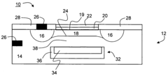
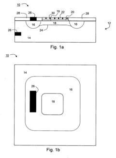
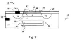
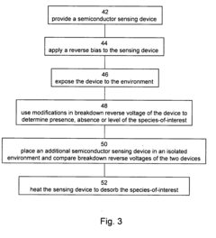
- A molecular controlled semiconductor sensing device is developed, featuring a device body with at least two semiconductor regions forming a p-n junction, where charge carrier concentrations are selected to achieve a predetermined reverse breakdown voltage, and molecules are deposited on the semiconductor material to interact with species-of-interest, modifying the breakdown voltage for sensitive and selective sensing.
PN junctions and methods
PatentActiveUS20120211747A1
Innovation
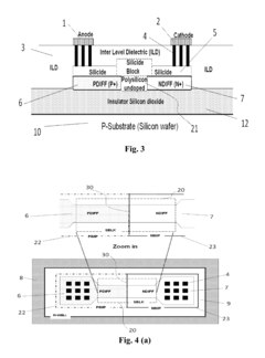
- The novel layout structures of 'saw-tooth' or 'wave' style P+ and N+ diffusion layers, which are partially overlapped, reduce misalignment sensitivity and ensure consistent cross-over regions for reliable current conduction, even under manufacturing errors, thereby improving manufacturability and yield.
Reliability and Lifetime Considerations in Breakdown Devices
The reliability and lifetime of breakdown devices, particularly when comparing P-N junctions and Zener diodes, represent critical considerations for electronic system designers. Breakdown phenomena, while functionally essential in voltage regulation applications, inherently stress semiconductor materials and can lead to accelerated aging or catastrophic failure if not properly managed.
Temperature effects significantly impact the long-term stability of breakdown devices. Zener diodes operating in the true Zener breakdown region (below approximately 5V) demonstrate a negative temperature coefficient, while those operating in avalanche breakdown exhibit positive temperature coefficients. This temperature sensitivity directly influences device lifetime, with thermal cycling causing mechanical stress at material interfaces and potentially leading to premature failure.
Current density during breakdown represents another crucial reliability factor. Excessive current concentration can create localized hot spots that accelerate electromigration processes, gradually degrading junction characteristics. Zener diodes are specifically engineered with larger junction areas and specialized doping profiles to distribute breakdown current more uniformly than standard P-N junctions, thereby enhancing their operational lifetime under repeated breakdown conditions.
Surface effects and passivation quality significantly influence breakdown device reliability. The junction termination regions are particularly vulnerable to contamination and mechanical stress. Modern Zener diodes incorporate specialized edge termination structures and passivation layers that substantially improve their resistance to environmental factors compared to basic P-N junctions, extending operational lifetime in harsh environments.
Predictive lifetime modeling for breakdown devices typically employs accelerated stress testing methodologies. Research indicates that Zener diodes designed specifically for breakdown operation can maintain stable voltage references for 15-20 years under proper operating conditions, while standard P-N junctions utilized in breakdown regions may exhibit significant parameter drift within 3-5 years.
Failure mechanisms in breakdown devices include junction heating, metal migration, oxide degradation, and package-related issues. Statistical analysis of these failure modes reveals that properly designed Zener diodes demonstrate mean time between failures (MTBF) rates approximately 5-10 times higher than standard P-N junctions when operated in breakdown regions, particularly under fluctuating load conditions.
Recent advances in semiconductor materials and fabrication techniques have significantly enhanced the reliability profiles of breakdown devices. Silicon carbide and gallium nitride-based breakdown devices demonstrate superior thermal performance and breakdown stability compared to traditional silicon implementations, potentially extending operational lifetimes by factors of 3-5 times in high-temperature applications.
Thermal Management Challenges in High-Power Breakdown Applications
The thermal management of high-power breakdown applications presents significant challenges when comparing P-N junction and Zener diode behaviors. During breakdown conditions, both device types experience substantial heat generation due to the high current flow and power dissipation. In P-N junctions, avalanche breakdown typically occurs at higher voltages and can spread across a wider area of the junction, distributing heat more evenly. However, this distribution is often insufficient to prevent localized hot spots that can lead to thermal runaway and catastrophic failure.
Zener diodes, specifically designed to operate in the breakdown region, incorporate specialized doping profiles and junction geometries to better handle the thermal stress. Despite these design optimizations, they still face significant thermal challenges when operating at high power levels. The concentrated nature of the breakdown current in Zener diodes can create intense thermal gradients that must be effectively managed to ensure reliable operation.
Heat dissipation mechanisms differ between these device types, with thermal conductivity pathways being critical design considerations. The package design and substrate materials significantly impact how efficiently heat can be removed from the active junction area. Silicon's relatively modest thermal conductivity (approximately 150 W/m·K) becomes a limiting factor in high-power applications, necessitating advanced packaging solutions or alternative semiconductor materials.
Temperature coefficients also play a crucial role in thermal stability. P-N junctions typically exhibit positive temperature coefficients during avalanche breakdown, meaning breakdown voltage increases with temperature. This characteristic helps distribute current more evenly across the junction. Zener diodes, depending on their breakdown voltage range, may exhibit either positive or negative temperature coefficients, with those operating below approximately 5V showing negative coefficients that can exacerbate thermal management challenges.
Advanced cooling strategies have evolved to address these thermal issues, including active cooling systems, thermally optimized packaging, and heat spreading structures. Die attachment methods using materials with high thermal conductivity, such as silver-filled epoxies or solder compounds, help improve heat transfer from the semiconductor to the package. In extreme high-power applications, direct liquid cooling or thermoelectric cooling may be employed to maintain junction temperatures within safe operating limits.
Thermal simulation and modeling have become essential tools in predicting device behavior under various operating conditions. Finite element analysis allows designers to identify potential hot spots and optimize thermal management solutions before physical prototyping. These simulations must account for the non-linear nature of breakdown behavior and the complex thermal interactions between the semiconductor, package, and surrounding environment.
Unlock deeper insights with Patsnap Eureka Quick Research — get a full tech report to explore trends and direct your research. Try now!
Generate Your Research Report Instantly with AI Agent
Supercharge your innovation with Patsnap Eureka AI Agent Platform!