Tungsten's Role In High-Temperature Electronics
Tungsten in Electronics: Background and Objectives
Tungsten has played a pivotal role in the development of high-temperature electronics, marking a significant milestone in the evolution of semiconductor technology. The journey of tungsten in this field began with its use in incandescent light bulbs, where its high melting point and durability made it an ideal filament material. As the electronics industry progressed, the unique properties of tungsten became increasingly valuable in more advanced applications.
The primary objective of incorporating tungsten in high-temperature electronics is to overcome the limitations of traditional semiconductor materials in extreme environments. Silicon-based devices typically fail at temperatures exceeding 150°C, whereas tungsten-based components can operate efficiently at temperatures well above 500°C. This capability opens up new possibilities for electronics in aerospace, automotive, and industrial sectors where high-temperature operation is critical.
Tungsten's exceptional thermal stability, low coefficient of thermal expansion, and high resistance to electromigration make it an excellent candidate for interconnects and gate electrodes in high-temperature semiconductor devices. Its ability to form stable silicides also enhances its compatibility with silicon-based technologies, facilitating integration into existing manufacturing processes.
The development of tungsten-based high-temperature electronics has been driven by the increasing demand for robust electronic systems in harsh environments. Applications such as deep-well drilling, jet engine control systems, and space exploration require electronics that can withstand extreme temperatures without compromising performance or reliability. Tungsten's unique properties address these challenges, enabling the creation of devices that maintain stability and functionality under severe thermal stress.
Recent advancements in thin-film deposition techniques and nanoscale engineering have further expanded the potential of tungsten in high-temperature electronics. Researchers are exploring novel tungsten-based alloys and composites to enhance its already impressive thermal and electrical properties. These developments aim to push the boundaries of operating temperatures even higher, potentially enabling electronics to function in environments previously thought impossible.
As we look towards the future, the role of tungsten in high-temperature electronics is expected to grow. The ongoing miniaturization of electronic devices and the increasing need for energy-efficient, high-performance systems in extreme conditions will continue to drive innovation in this field. Tungsten's unique characteristics position it as a key material in the development of next-generation high-temperature electronic components, promising to revolutionize industries that operate in challenging thermal environments.
Market Analysis for High-Temperature Electronics
The high-temperature electronics market has been experiencing significant growth due to increasing demand across various industries. This sector primarily caters to applications that require electronic components to function reliably in extreme temperature environments, typically above 150°C. The market is driven by the expanding needs of aerospace, automotive, oil and gas, and industrial sectors.
In the aerospace industry, high-temperature electronics are crucial for engine control systems, flight control actuators, and sensor networks. The automotive sector utilizes these components in engine management systems, exhaust gas sensors, and brake control units. The oil and gas industry relies on high-temperature electronics for downhole drilling tools, well logging equipment, and geothermal exploration. Industrial applications include power electronics, furnace controls, and nuclear power plant instrumentation.
Market research indicates that the global high-temperature electronics market is projected to grow at a compound annual growth rate (CAGR) of over 8% from 2021 to 2026. This growth is attributed to the increasing adoption of electric vehicles, the expansion of renewable energy systems, and the ongoing development of more efficient and durable electronic components for harsh environments.
Tungsten plays a critical role in this market due to its exceptional high-temperature properties. As a refractory metal with the highest melting point of all elements, tungsten is ideal for use in high-temperature electronic applications. It is commonly used in the fabrication of electrodes, interconnects, and heat sinks in high-temperature electronic devices.
The demand for tungsten in high-temperature electronics is expected to rise in parallel with the overall market growth. This is particularly evident in the development of wide bandgap semiconductors, such as silicon carbide (SiC) and gallium nitride (GaN), which are capable of operating at higher temperatures than traditional silicon-based devices. Tungsten's compatibility with these advanced semiconductor materials further enhances its importance in the high-temperature electronics ecosystem.
Key market players in the high-temperature electronics sector include Texas Instruments, Honeywell International, BAE Systems, and Analog Devices. These companies are investing heavily in research and development to create more robust and efficient high-temperature electronic solutions, often incorporating tungsten-based components in their designs.
As industries continue to push the boundaries of operational environments, the demand for high-temperature electronics is expected to grow, subsequently driving the need for tungsten and other refractory materials. This trend is likely to create new opportunities for material suppliers, component manufacturers, and system integrators in the high-temperature electronics value chain.
Current State and Challenges of Tungsten-Based Electronics
Tungsten-based electronics have made significant strides in recent years, particularly in high-temperature applications. The current state of this technology is characterized by a growing understanding of tungsten's unique properties and its potential to revolutionize electronics in extreme environments. Tungsten's high melting point, excellent thermal conductivity, and resistance to corrosion make it an ideal candidate for electronic components that must operate under severe conditions.
One of the primary challenges in tungsten-based electronics is the integration of tungsten with other materials in semiconductor devices. While tungsten's properties are advantageous, its compatibility with traditional silicon-based manufacturing processes is limited. Researchers are actively working on developing new fabrication techniques and material combinations to overcome these integration issues.
Another significant challenge lies in the development of stable and reliable tungsten-based thin films. These films are crucial for creating interconnects and electrodes in high-temperature electronic devices. Current research focuses on improving the deposition methods and controlling the microstructure of tungsten films to enhance their performance and longevity under extreme conditions.
The miniaturization of tungsten-based components presents another hurdle. As electronic devices continue to shrink, maintaining the performance of tungsten elements at smaller scales becomes increasingly difficult. This challenge is particularly pronounced in the development of nanoscale tungsten structures for advanced electronic applications.
Thermal management remains a critical issue in tungsten-based electronics. While tungsten's high thermal conductivity is beneficial, designing efficient heat dissipation systems for compact, high-power devices is complex. Engineers are exploring innovative cooling solutions and thermal interface materials to address this challenge.
The development of tungsten-based power electronics is an area of intense research. Tungsten's potential in high-voltage and high-current applications is promising, but challenges persist in creating reliable and efficient power devices that can withstand extreme temperatures and electrical stresses.
Lastly, the cost and complexity of manufacturing tungsten-based electronics pose significant challenges to widespread adoption. Current production methods are often expensive and time-consuming, limiting the technology's commercial viability. Efforts are underway to develop more cost-effective manufacturing processes and to identify potential economies of scale.
Despite these challenges, the field of tungsten-based electronics continues to advance. Ongoing research and development are focused on overcoming these obstacles, with promising results emerging in areas such as aerospace, deep-earth exploration, and nuclear power applications. As solutions to these challenges are developed, tungsten-based electronics are poised to play an increasingly important role in enabling next-generation high-temperature electronic systems.
Existing Tungsten Applications in High-Temperature Electronics
01 Tungsten deposition methods
Various methods for depositing tungsten on substrates, including chemical vapor deposition (CVD) and atomic layer deposition (ALD). These techniques are used to create thin films of tungsten for applications in semiconductor manufacturing and other industries.- Tungsten deposition and film formation: Various methods and processes for depositing tungsten and forming tungsten films on substrates. This includes techniques such as chemical vapor deposition (CVD), atomic layer deposition (ALD), and physical vapor deposition (PVD) to create thin films of tungsten for use in semiconductor devices and other applications.
- Tungsten alloys and composites: Development of tungsten alloys and composite materials that combine tungsten with other elements or compounds to enhance specific properties. These materials may offer improved strength, hardness, thermal stability, or electrical conductivity for use in various industrial applications.
- Tungsten in semiconductor manufacturing: Use of tungsten in semiconductor manufacturing processes, including its application as interconnects, gate electrodes, and contact materials. This involves techniques for patterning, etching, and integrating tungsten into complex semiconductor structures to improve device performance and reliability.
- Tungsten-based lighting and electron emission: Applications of tungsten in lighting technologies and electron emission devices. This includes the use of tungsten filaments in incandescent lamps, cathodes in electron tubes, and field emission devices. The focus is on optimizing tungsten properties for improved efficiency and longevity in these applications.
- Recycling and processing of tungsten: Methods for recycling and processing tungsten from various sources, including scrap materials and end-of-life products. This involves techniques for extracting, purifying, and recovering tungsten to create high-quality raw materials for reuse in industrial applications, promoting sustainability and resource efficiency.
02 Tungsten etching processes
Techniques for selectively removing tungsten from surfaces, often used in semiconductor fabrication. These processes may involve chemical or plasma etching to create specific patterns or structures in tungsten layers.Expand Specific Solutions03 Tungsten-based alloys and composites
Development of materials that combine tungsten with other elements to enhance properties such as strength, conductivity, or heat resistance. These alloys and composites find applications in various industries, including aerospace and electronics.Expand Specific Solutions04 Tungsten in electrical components
Use of tungsten in the manufacture of electrical components, such as filaments, electrodes, and interconnects. Tungsten's high melting point and good electrical conductivity make it suitable for these applications.Expand Specific Solutions05 Tungsten surface treatment and modification
Processes for modifying the surface properties of tungsten, including cleaning, polishing, and functionalization. These treatments can improve the material's performance in specific applications or prepare it for further processing steps.Expand Specific Solutions
Key Players in Tungsten-Based Electronics Industry
The high-temperature electronics market, driven by tungsten's unique properties, is in a growth phase with increasing demand across various industries. The market size is expanding, fueled by applications in aerospace, automotive, and energy sectors. Technologically, the field is advancing rapidly, with companies like Applied Materials, Inc., Toshiba Corp., and Siemens Corp. leading innovation. These firms are developing advanced tungsten-based solutions for high-temperature electronic components. Research institutions such as the University of Science & Technology Beijing and Beijing University of Technology are contributing to fundamental advancements. The competitive landscape is characterized by a mix of established electronics giants and specialized materials companies, with ongoing research collaborations driving technological maturity and market expansion.
Applied Materials, Inc.
Toshiba Corp.
Core Innovations in Tungsten-Based Electronic Components
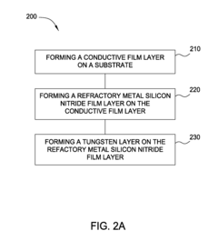
- A CVD chamber system that supports substrates at varying distances from the heater to maintain different temperatures within a single processing chamber, allowing for both nucleation and bulk tungsten deposition processes to be performed without transferring the substrate, using a shadow ring lift assembly and light pipe for temperature determination and control.
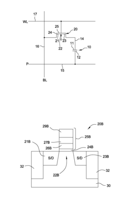
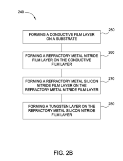
- A gate electrode stack is formed using a refractory metal silicon nitride film layer and a tungsten film layer, where the refractory metal silicon nitride film is deposited using a titanium-silicon alloy target in an Ar/N2 environment, reducing the number of processing chambers required and minimizing exposure to contaminants, thereby lowering the resistivity of the tungsten film.
Environmental Impact of Tungsten in Electronics Manufacturing
The environmental impact of tungsten in electronics manufacturing is a critical consideration as the demand for high-temperature electronic components continues to grow. Tungsten, known for its exceptional thermal properties and high melting point, plays a crucial role in advanced electronic systems. However, its extraction, processing, and disposal pose significant environmental challenges.
Mining and extraction of tungsten ore can lead to habitat destruction, soil erosion, and water pollution. The process often involves large-scale excavation, which disrupts local ecosystems and can contaminate nearby water sources with heavy metals and other pollutants. Additionally, the energy-intensive nature of tungsten extraction contributes to increased carbon emissions, exacerbating climate change concerns.
In the manufacturing phase, tungsten processing requires substantial energy inputs and often involves the use of hazardous chemicals. The production of tungsten carbide, a common form used in electronics, generates toxic dust and fumes that can pose health risks to workers and nearby communities if not properly managed. Furthermore, the high temperatures required for tungsten processing contribute to increased energy consumption and associated greenhouse gas emissions.
The use of tungsten in electronic components also raises concerns about electronic waste (e-waste) management. As electronic devices reach the end of their life cycle, proper disposal and recycling of tungsten-containing components become crucial. Improper handling of e-waste can lead to the release of toxic substances into the environment, potentially contaminating soil and water resources.
However, efforts are being made to mitigate the environmental impact of tungsten in electronics manufacturing. Recycling initiatives aim to recover tungsten from used electronic components, reducing the need for new raw material extraction. Advanced manufacturing techniques are being developed to minimize waste and improve energy efficiency in tungsten processing.
Research into alternative materials and more sustainable production methods is ongoing. Some companies are exploring bio-based alternatives or developing more environmentally friendly extraction processes. Additionally, stricter regulations and industry standards are being implemented to ensure responsible sourcing and manufacturing practices.
As the electronics industry continues to evolve, balancing the technological benefits of tungsten with environmental sustainability remains a key challenge. Addressing these environmental concerns will be crucial for the long-term viability of tungsten in high-temperature electronics applications.
Reliability Testing for Tungsten-Based Electronic Devices
Reliability testing for tungsten-based electronic devices is a critical aspect of ensuring the performance and longevity of high-temperature electronics. These tests are designed to evaluate the devices' ability to withstand extreme conditions and maintain functionality over extended periods.
One of the primary reliability tests for tungsten-based devices is thermal cycling. This test subjects the components to repeated cycles of extreme temperature changes, typically ranging from -55°C to 150°C or higher. The purpose is to assess the device's ability to withstand thermal expansion and contraction without experiencing mechanical failure or performance degradation.
High-temperature storage tests are another crucial aspect of reliability testing. In these tests, devices are exposed to elevated temperatures, often exceeding 200°C, for extended periods. This helps evaluate the long-term stability of the tungsten-based components and identifies any potential issues related to material degradation or chemical reactions at high temperatures.
Accelerated life testing is employed to simulate years of operation in a compressed timeframe. This involves subjecting the devices to conditions that are more severe than typical operating environments, such as higher temperatures or voltages. The results are then extrapolated to predict the expected lifespan of the devices under normal operating conditions.
Humidity and moisture resistance tests are also conducted to assess the devices' ability to function in high-humidity environments. While tungsten itself is resistant to moisture, other components in the device may be susceptible to corrosion or performance issues in humid conditions.
Mechanical stress tests, including vibration and shock testing, are performed to evaluate the robustness of tungsten-based devices in applications where they may be subjected to physical stresses. These tests help ensure that the devices can withstand the rigors of transportation and operation in harsh environments.
Electrical stress testing is another critical component of reliability assessment. This involves subjecting the devices to voltage and current levels beyond their normal operating range to identify potential failure modes and determine safe operating limits.
Finally, radiation hardness testing is often conducted for tungsten-based devices intended for use in aerospace or nuclear applications. These tests evaluate the devices' ability to maintain functionality when exposed to various types of radiation, including gamma rays and high-energy particles.
The results of these comprehensive reliability tests are used to refine device designs, improve manufacturing processes, and provide accurate specifications for end-users. This ensures that tungsten-based electronic devices can meet the demanding requirements of high-temperature applications across various industries.