Ultrafast Laser Annealing in Advanced Coating Systems
OCT 10, 202510 MIN READ
Generate Your Research Report Instantly with AI Agent
Patsnap Eureka helps you evaluate technical feasibility & market potential.
Ultrafast Laser Annealing Background and Objectives
Ultrafast laser annealing represents a significant advancement in materials processing technology, particularly for advanced coating systems. This technique has evolved over the past three decades from a laboratory curiosity to an essential industrial process. The fundamental principle involves the application of ultra-short laser pulses (typically in the femtosecond to picosecond range) to rapidly heat material surfaces without causing thermal damage to underlying substrates.
The historical development of ultrafast laser annealing began in the 1990s with the commercialization of reliable femtosecond laser systems. Initial applications focused primarily on semiconductor processing, but by the early 2000s, researchers began exploring applications in thin-film coatings. The technology gained significant momentum after 2010 when advances in laser stability and beam control enabled precise energy delivery to complex coating architectures.
Current technological trends indicate a shift toward higher processing speeds, greater precision, and integration with in-line manufacturing systems. The miniaturization of laser systems and development of multi-beam processing approaches are enabling broader industrial adoption. Additionally, there is growing interest in combining ultrafast laser annealing with other surface modification techniques to create hybrid processing solutions.
The primary objectives of ultrafast laser annealing in advanced coating systems include enhancing coating adhesion, improving wear resistance, modifying optical properties, and enabling novel functionalities through controlled microstructural changes. Specifically, the technology aims to achieve localized annealing without thermal damage to temperature-sensitive substrates—a capability not possible with conventional thermal processing methods.
Another critical objective is to develop energy-efficient annealing processes that can be scaled for industrial production. This includes optimizing laser parameters (pulse duration, repetition rate, fluence) for specific coating materials and thicknesses. The technology also seeks to enable the processing of increasingly complex multi-layer coating systems where selective modification of individual layers is required.
From a materials science perspective, ultrafast laser annealing aims to control phase transformations, crystallization processes, and interfacial reactions with unprecedented temporal and spatial precision. This capability opens new possibilities for creating metastable phases and unique microstructures that cannot be achieved through conventional processing routes.
Looking forward, the field is moving toward real-time process monitoring and closed-loop control systems that can adjust laser parameters dynamically based on material response. The integration of machine learning algorithms for process optimization represents another frontier, potentially enabling autonomous optimization of annealing parameters for novel coating compositions.
Market Demand Analysis for Advanced Coating Systems
The global market for advanced coating systems has witnessed substantial growth in recent years, driven by increasing demands across multiple industries for enhanced material performance. The integration of ultrafast laser annealing technology into coating processes represents a significant advancement that addresses critical market needs for precision, efficiency, and material quality enhancement.
The automotive sector demonstrates particularly strong demand for advanced coating systems, with projections indicating a compound annual growth rate of 6.8% through 2028. This growth is primarily fueled by requirements for corrosion resistance, thermal management, and aesthetic finishes that can withstand harsh environmental conditions while reducing overall vehicle weight. Ultrafast laser annealing offers precise control over coating properties that traditional thermal processing cannot achieve.
In the electronics industry, the miniaturization trend continues to drive demand for increasingly sophisticated coating solutions. The semiconductor market specifically requires nanometer-precision coatings with perfect uniformity, where ultrafast laser annealing provides significant advantages over conventional methods. Market analysis reveals that approximately 40% of advanced semiconductor manufacturing facilities are exploring laser-based coating technologies to meet next-generation device requirements.
The aerospace sector represents another significant market segment, valued at approximately $3.2 billion for specialized coating systems. Here, the demand centers on thermal barrier coatings and protective layers that can withstand extreme temperature fluctuations and mechanical stress. Ultrafast laser annealing enables the development of multi-functional coatings with superior adhesion and durability characteristics that conventional processes cannot match.
Medical device manufacturing has emerged as a rapidly growing application area, with particular emphasis on biocompatible coatings for implantable devices. This segment is experiencing annual growth exceeding 9%, driven by increasing procedural volumes and stricter regulatory requirements for device performance and safety. Ultrafast laser annealing provides the precision needed for these critical applications while minimizing thermal damage to sensitive substrates.
Energy sector applications, particularly in solar panel manufacturing and battery technologies, represent an expanding market opportunity. The demand for higher efficiency energy conversion and storage systems has created requirements for specialized coatings that can be precisely engineered at the molecular level. Market research indicates that companies investing in advanced coating technologies achieve up to 15% improvements in product performance metrics.
Regional analysis shows Asia-Pacific leading market growth, accounting for approximately 45% of global demand, followed by North America and Europe. This distribution reflects the concentration of electronics manufacturing in Asia, automotive production across all three regions, and aerospace development primarily in North America and Europe.
Current State and Challenges in Laser Annealing Technology
Ultrafast laser annealing technology has witnessed significant advancements globally, with major research centers in North America, Europe, and East Asia leading innovation efforts. The United States maintains technological leadership through institutions like Lawrence Berkeley National Laboratory and companies such as Applied Materials, while European research clusters in Germany and Switzerland focus on precision applications. Japan and South Korea have established strong positions in semiconductor-related laser annealing processes, with companies like Tokyo Electron and Samsung developing proprietary solutions.
The current state of ultrafast laser annealing in advanced coating systems represents a complex technological landscape characterized by both remarkable achievements and persistent challenges. Modern systems typically employ femtosecond and picosecond lasers operating at pulse durations below 10 picoseconds, enabling precise energy delivery without excessive heat diffusion into surrounding materials. This capability has revolutionized thin-film processing in semiconductor manufacturing, allowing for localized annealing without compromising adjacent structures.
Despite these advances, several significant technical challenges continue to impede broader industrial adoption. Scaling ultrafast laser annealing for high-volume manufacturing remains problematic due to throughput limitations. Current systems struggle to process large surface areas efficiently while maintaining the precision required for advanced coating applications. This throughput bottleneck represents a major constraint for industries requiring mass production capabilities.
Energy efficiency presents another substantial challenge, as ultrafast laser systems typically demonstrate conversion efficiencies below 30%. This inefficiency translates to higher operational costs and environmental impact, limiting economic viability for certain applications. Additionally, the complex optical systems required for beam delivery and manipulation contribute to high equipment costs and maintenance requirements.
Process control and uniformity issues persist across varied substrate geometries and material compositions. Achieving consistent annealing results across three-dimensional structures with complex topographies remains particularly challenging. Real-time monitoring and feedback systems have improved but still lack the precision needed for the most demanding applications in advanced coating systems.
Material-specific challenges further complicate implementation, as different coating materials respond uniquely to ultrafast laser exposure. Engineers must carefully calibrate parameters for each material system, creating significant complexity in multi-layer coating applications. The interaction between ultrafast laser pulses and novel advanced coating materials, particularly nanostructured composites, remains incompletely understood, necessitating further fundamental research.
Integration with existing manufacturing workflows represents a practical challenge, as ultrafast laser annealing systems must coexist with established processes. This integration often requires significant reconfiguration of production lines and development of specialized interfaces, creating barriers to adoption for manufacturers with established infrastructure.
Current Technical Solutions for Ultrafast Laser Annealing
01 Semiconductor device manufacturing using ultrafast laser annealing
Ultrafast laser annealing is used in semiconductor manufacturing to modify material properties without causing thermal damage to surrounding areas. The technique employs femtosecond or picosecond lasers to precisely anneal specific regions of semiconductor wafers, enabling the creation of high-performance electronic devices. This process allows for localized heating and rapid cooling, which is crucial for advanced node semiconductor fabrication where precise control of dopant activation and crystal structure is required.- Semiconductor device manufacturing using ultrafast laser annealing: Ultrafast laser annealing is used in semiconductor manufacturing to modify material properties without causing thermal damage to surrounding areas. The process involves using ultrashort laser pulses to rapidly heat and cool semiconductor materials, enabling precise doping, crystallization, and defect repair. This technique is particularly valuable for advanced node technologies where thermal budgets are constrained and precise control of material properties is critical.
- Materials processing with ultrafast laser annealing: Ultrafast laser annealing enables precise modification of various materials including metals, glasses, and polymers. The technique allows for localized heating that can alter material properties such as hardness, conductivity, and optical characteristics without affecting the bulk material. Applications include surface hardening, creating conductive paths in non-conductive materials, and modifying optical properties for specialized applications.
- Optical device fabrication using ultrafast laser annealing: Ultrafast laser annealing is employed in the fabrication of optical devices such as waveguides, optical fibers, and photonic integrated circuits. The technique allows for precise modification of refractive indices in transparent materials, enabling the creation of complex optical structures. The non-thermal nature of ultrafast laser processing prevents unwanted thermal effects that could compromise optical performance.
- Medical applications of ultrafast laser annealing: Ultrafast laser annealing has applications in medical device manufacturing and treatments. The precision of ultrafast lasers allows for minimally invasive procedures, tissue modification with minimal thermal damage, and fabrication of biocompatible implants. The technique enables precise cutting, welding, and surface modification of medical materials while maintaining biocompatibility and structural integrity.
- Advanced laser system configurations for ultrafast annealing: Specialized laser systems have been developed specifically for ultrafast annealing applications. These systems incorporate features such as precise pulse shaping, beam steering technologies, and sophisticated control systems to optimize the annealing process. Innovations include multi-beam processing, spatial light modulators for beam patterning, and feedback systems that monitor and adjust processing parameters in real-time to ensure consistent results.
02 Ultrafast laser annealing for material processing
Ultrafast laser annealing techniques are applied to various materials for surface modification, crystallization, and property enhancement. The process involves using short-pulse lasers to rapidly heat material surfaces without significant heat diffusion to the bulk, allowing for precise microstructural changes. This approach is particularly valuable for processing temperature-sensitive materials, creating specialized surface properties, or inducing phase transformations that would be impossible with conventional heating methods.Expand Specific Solutions03 Optical device fabrication using ultrafast laser annealing
Ultrafast laser annealing is employed in the fabrication and modification of optical devices such as waveguides, photonic integrated circuits, and optical fibers. The technique allows for precise refractive index modification, creation of optical gratings, and formation of active regions in photonic devices. By using ultrafast lasers, manufacturers can achieve highly localized modifications to optical materials without causing unwanted thermal effects that could degrade device performance.Expand Specific Solutions04 Ultrafast laser systems and control methods
Advanced ultrafast laser systems have been developed specifically for annealing applications, featuring precise control of pulse characteristics, beam delivery, and scanning patterns. These systems incorporate sophisticated optics, beam shaping technologies, and control algorithms to achieve uniform energy distribution and consistent processing results. Innovations in this area focus on improving laser stability, increasing processing speed, and enhancing the flexibility of ultrafast laser annealing systems for various industrial applications.Expand Specific Solutions05 Medical and biological applications of ultrafast laser annealing
Ultrafast laser annealing has found applications in medical device manufacturing and biological tissue processing. The technique enables precise modification of biomaterials, creation of specialized surface textures on medical implants, and controlled tissue ablation with minimal thermal damage. The ultra-short pulse duration allows for high-precision processing of heat-sensitive biological materials and can be used for creating microstructures that enhance biocompatibility or drug delivery capabilities.Expand Specific Solutions
Key Industry Players in Advanced Coating and Laser Systems
Ultrafast Laser Annealing in Advanced Coating Systems is currently in a growth phase, with the market expanding due to increasing applications in semiconductor manufacturing, display technologies, and advanced materials processing. The global market is estimated to reach several billion dollars by 2025, driven by demand for higher-efficiency electronic components and advanced display technologies. Technologically, the field is in mid-maturity, with established players like Coherent, Inc. and IMRA America leading innovation in ultrafast laser systems, while companies such as BOE Technology, Samsung Electronics, and Veeco Instruments are advancing implementation in production environments. Research institutions including Fraunhofer-Gesellschaft and Naval Research Laboratory continue to push boundaries in fundamental laser-material interaction science. Japanese manufacturers like Gigaphoton and FUJIFILM are particularly strong in specialized coating applications, while Chinese entities such as BOE and Beijing U-PRECISION TECH are rapidly gaining technological competence.
Veeco Instruments, Inc.
Technical Solution: Veeco Instruments has developed advanced ultrafast laser annealing technology specifically designed for precision coating applications in semiconductor and advanced packaging industries. Their system utilizes a hybrid approach combining ultrafast laser pulses (typically 5-20ps duration) with sophisticated beam shaping optics to achieve highly uniform energy distribution. Veeco's proprietary LSA (Laser Spike Annealing) technology enables millisecond-scale thermal processing with temperature ramp rates exceeding 10⁶°C/s, allowing for precise microstructural control of thin films without affecting underlying temperature-sensitive layers. Their systems incorporate advanced optical scanning technology that maintains consistent beam characteristics across large processing areas up to 300mm wafers. Veeco has also developed specialized process recipes for various coating materials including metal films, dielectrics, and compound semiconductors, optimizing parameters like dwell time, peak temperature, and cooling rate for each material system. Their latest generation systems feature in-situ metrology capabilities including thermal imaging and reflectivity measurements that provide real-time feedback on the annealing process, enabling closed-loop control for enhanced repeatability and yield.
Strengths: Exceptional temperature control precision (±5°C) across the processing area; demonstrated capability for selective annealing of complex multi-layer stacks; comprehensive process development support with material-specific optimization. Weaknesses: Systems primarily optimized for wafer-level processing rather than large-area applications; higher capital and operating costs compared to conventional rapid thermal annealing; requires specialized technical expertise for process development and system maintenance.
Coherent, Inc.
Technical Solution: Coherent has developed advanced ultrafast laser annealing systems specifically designed for coating applications. Their technology utilizes femtosecond and picosecond lasers that deliver extremely short pulses (typically <10 picoseconds) with high peak powers exceeding 10 GW/cm². This enables precise thermal processing of thin films and coatings without damaging underlying substrates. Coherent's systems incorporate proprietary beam shaping technology that ensures uniform energy distribution across the processing area, critical for consistent annealing results. Their latest platforms feature real-time process monitoring with integrated spectroscopy capabilities that analyze material changes during annealing, allowing for closed-loop control of the process parameters. Coherent has also pioneered multi-beam processing techniques that significantly increase throughput while maintaining precision, making their systems suitable for high-volume manufacturing environments in semiconductor, display, and photovoltaic industries.
Strengths: Superior pulse control technology enabling precise energy delivery to target layers without thermal damage to adjacent materials; advanced beam shaping capabilities ensuring uniform treatment across large areas; integrated process monitoring for quality control. Weaknesses: Higher initial capital investment compared to conventional annealing methods; requires specialized technical expertise for operation and maintenance; limited processing depth for certain thick coating applications.
Core Patents and Research in Ultrafast Laser-Material Interaction
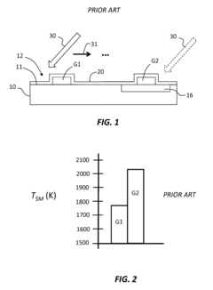
Ultrafast laser annealing with reduced pattern density effects in integrated circuit fabrication
PatentInactiveUS9302348B2
Innovation
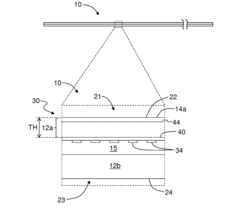
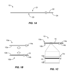
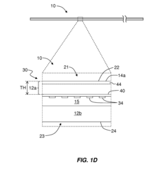
- The method involves using a first laser beam to preheat the patterned surface to a non-melt temperature within 400°C of the melt temperature, followed by a second pulsed laser beam to raise the temperature to the melt temperature, optimizing the temperature variation and reducing pattern density effects.
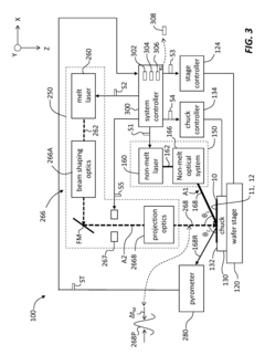
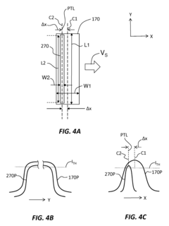
Laser annealing systems and methods with ultra-short dwell times
PatentActiveUS20160240407A9
Innovation
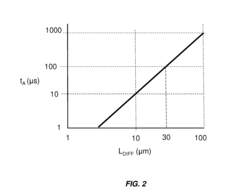
- The development of ultra-fast laser annealing systems using one or two laser beams that overlap, with a primary and secondary laser system, where the secondary laser scans the wafer surface at dwell times between 1 μs and 100 μs, achieving a peak annealing temperature between 350° C. and 1250° C. while maintaining temperature uniformity within ±3° C., utilizing a thermal emission detector and controller to adjust power and ensure consistent annealing.
Energy Efficiency and Sustainability Considerations
Ultrafast laser annealing in advanced coating systems presents significant opportunities for enhancing energy efficiency and sustainability across multiple industrial applications. The process fundamentally reduces energy consumption compared to conventional thermal annealing methods, with studies indicating energy savings of 30-60% depending on the specific coating material and substrate combination. This efficiency stems from the highly targeted nature of ultrafast laser energy delivery, which minimizes waste heat and reduces the total processing time from hours to minutes or even seconds.
From a lifecycle assessment perspective, ultrafast laser annealing demonstrates remarkable sustainability advantages. The reduced processing temperatures and times translate directly to lower carbon footprints, with recent industry analyses showing potential CO2 emission reductions of up to 45% compared to conventional annealing processes. Additionally, the precision of ultrafast laser systems minimizes material waste through optimized energy distribution and reduced need for post-processing treatments.
The technology enables the development of more environmentally friendly coating formulations by eliminating the need for certain harmful solvents and additives typically required for conventional thermal processing. This aspect is particularly relevant in sectors like consumer electronics and automotive manufacturing, where regulatory pressures for greener manufacturing processes continue to intensify.
Energy recovery systems integrated with ultrafast laser annealing equipment represent another frontier in sustainability enhancement. Advanced thermal management designs can capture and repurpose up to 25% of the energy typically lost during processing, further improving the overall efficiency metrics. Several leading equipment manufacturers have begun incorporating these recovery systems as standard features in their latest generation of industrial laser annealing platforms.
The scalability of ultrafast laser annealing contributes significantly to its sustainability profile. Unlike conventional batch processing methods, laser-based systems can be more easily adapted to variable production volumes, reducing idle energy consumption during periods of lower demand. This flexibility translates to optimized energy utilization across the production lifecycle and supports leaner manufacturing approaches.
Long-term durability improvements in coatings processed via ultrafast laser annealing further enhance the sustainability equation. Enhanced coating performance extends product lifespans by 15-30% according to accelerated aging tests, reducing replacement frequency and associated resource consumption. This aspect is particularly valuable in applications exposed to harsh environmental conditions, such as outdoor architectural coatings and marine protective systems.
Materials Compatibility and Process Integration Challenges
The integration of ultrafast laser annealing technology with advanced coating systems presents significant materials compatibility challenges that must be addressed for successful industrial implementation. Different coating materials exhibit varying thermal properties, absorption characteristics, and phase transformation behaviors when subjected to ultrafast laser pulses. For instance, metallic coatings typically demonstrate high thermal conductivity and reflectivity, while ceramic coatings show lower thermal conductivity but may be prone to thermal shock under rapid heating conditions. These inherent material differences necessitate careful parameter optimization to prevent delamination, cracking, or undesired microstructural changes at interfaces.
Multi-layer coating systems introduce additional complexity due to thermal expansion coefficient mismatches between adjacent layers. When exposed to the extreme temperature gradients characteristic of ultrafast laser annealing, these mismatches can generate substantial interfacial stresses. Research indicates that stress accumulation at interfaces can lead to coating failure even when individual layers remain intact, particularly in applications requiring thermal cycling or mechanical loading during service.
Substrate-coating interactions further complicate process integration. The thermal energy transferred through the coating to the substrate can trigger diffusion processes, potentially compromising coating adhesion or altering substrate properties. This is especially problematic for temperature-sensitive substrates such as polymers or certain electronic components, where even brief thermal excursions can cause degradation or functional failure.
Process integration challenges extend beyond materials compatibility to include manufacturing workflow considerations. Ultrafast laser annealing must be positioned appropriately within the coating production sequence. Introducing this process after certain surface treatments may nullify their effects, while performing it too early might necessitate additional protective measures during subsequent processing steps. The equipment footprint, throughput capabilities, and environmental control requirements also impact integration feasibility in existing production lines.
Quality control and process monitoring present additional hurdles. The rapid, localized nature of ultrafast laser annealing makes real-time temperature measurement challenging, complicating process validation and repeatability assurance. Non-destructive evaluation techniques must be adapted or developed to verify coating integrity post-annealing without compromising production efficiency.
Environmental and safety considerations also influence integration strategies. Laser processing may generate particulates or vapors depending on coating composition, requiring appropriate extraction and filtration systems. Additionally, the high-power laser equipment necessitates robust safety protocols and potentially specialized facility modifications to ensure operator protection and regulatory compliance.
Unlock deeper insights with Patsnap Eureka Quick Research — get a full tech report to explore trends and direct your research. Try now!
Generate Your Research Report Instantly with AI Agent
Supercharge your innovation with Patsnap Eureka AI Agent Platform!