Semiconductor machine

A semiconductor and machine technology, applied in the field of semiconductor machines, can solve problems such as the difficulty of probe 171, and achieve the effect of shortening the warm-up time

CN100353516CInactive Publication Date: 2007-12-05POWERCHIP SEMICON CORP
5 Cites 0 Cited by

Patent Information

Authority / Receiving Office
CN · China
Patent Type
Patents(China)
Current Assignee / Owner
Publication Date
2007-12-05
Estimated Expiration
Not applicable · inactive patent

Smart Images

  • Figure 1
    Figure 1
  • Figure 2
    Figure 2
  • Figure 3
    Figure 3
Patent Text Reader

Abstract

The semiconductor machine bench comprises a printed circuit board with first and second surfaces, a heat source to stable provide heat for the first liquid near circuit board to heat the board, and a regulating device to control the temperature of first surface to under the second surface and make the board deformation achieve rapidly stable state.
Need to check novelty before this filing date? Find Prior Art

Description

Technical field:

[0001] The invention relates to a semiconductor machine, in particular to a wafer testing machine. Background technique:

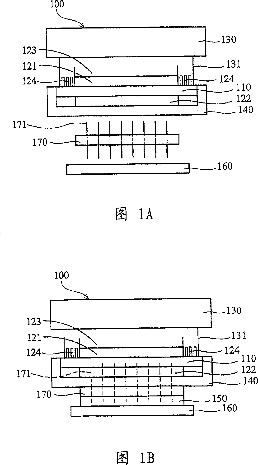
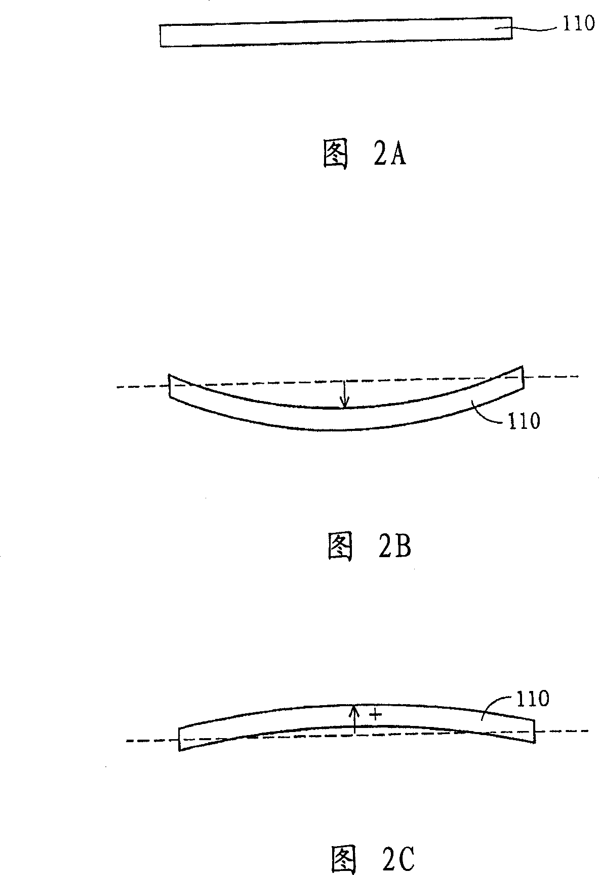
[0002] Referring to FIG. 1A, it shows a test head 100 of a conventional wafer testing machine, which has a test head body 130, a first restraint 121, a second restraint 122, a printed circuit board 110, a clamping member 140 and a probe base 170 . The first restraining member 121 and the second restraining member 122 clamp the printed circuit board 110 to limit the degree of deformation of the printed circuit board 110, and the connecting part 131 and the printed circuit board 110 pass through the positioning part 124 (this embodiment adopts ZIF Connected by zero insertion force socket) to provide mutual fixation. The test head body 130 is connected to the printed circuit board 110 through the connecting portion 131 . The clamping part 140 clamps the printed circuit board 110 . The crystal base 160 is disposed under the test head 100...

Examples

Embodiment Construction

[0040] Referring to FIG. 4 , it shows the semiconductor tool of the present invention, which has a test head 100 and a wafer base 160 . The test head 100 has a test head body 130 , a first restraint 121 , a second restraint 122 , a printed circuit board 110 , a clamp 140 , a probe holder 170 and an adjustment device 180 . The first restraining member 121 and the second restraining member 122 clamp the printed circuit board 110 to limit the degree of deformation of the printed circuit board 110, and the connecting part 131 and the printed circuit board 110 pass through the positioning part 124 (this embodiment adopts ZIF zero plug-in force socket connection) to provide mutual fixation. The test head body 130 is connected to the printed circuit board 110 through the connecting portion 131 . The regulating device 180 protrudes into the test head body 130 , and guides the airflow into the first constraining part 121 through the heat dissipation part 123 to regulate the surface te...