Light emitting device with fluorescent material
A fluorescent substance and ultraviolet light technology, applied in semiconductor devices, electrical components, circuits, etc., can solve problems such as shortening the light emission wavelength, difficulty in high-efficiency and high-color reproduction light-emitting devices, and low light emission efficiency of red fluorescent substances
- Summary
- Abstract
- Description
- Claims
- Application Information
AI Technical Summary
Problems solved by technology
Method used
Image


Examples
no. 1 example
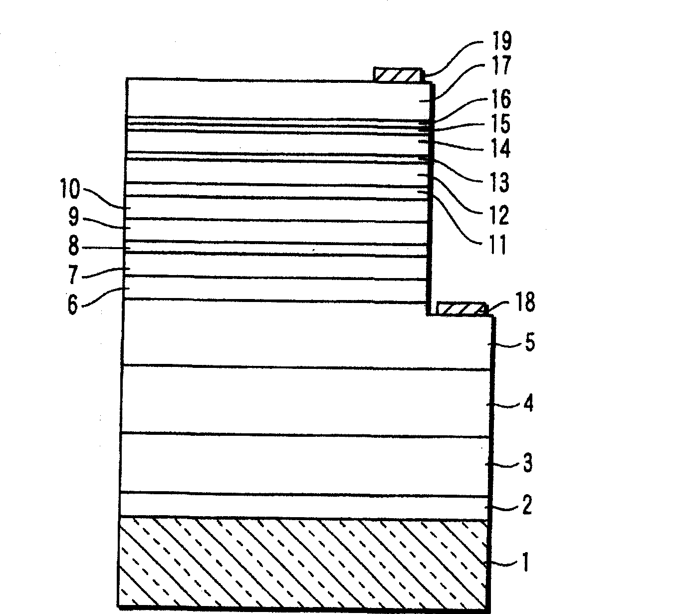
[0022] Such as figure 1 As shown in , the light emitting device according to this embodiment is a light emitting diode formed of a GaN-based compound semiconductor formed on a sapphire substrate. That is, on a substrate 1 whose surface is a sapphire c-plane, a first AlN buffer layer 2 having a high carbon concentration (carbon concentration: 3×10 18 up to 5×10 20 / cm 3 , film thickness: 3 to 20nm), high-purity second AlN buffer layer 3 (carbon concentration: 1×10 18 to 3×10 18 / cm 3 , film thickness: 2 μm), non-doped GaN buffer layer 4 (film thickness: 3 μm), Si-doped n-type GaN contact layer 5 (Si concentration: 1×10 18 up to 5×10 18 / cm 3 , film thickness: 2 to 5 μm).
[0023] In addition, on the Si-doped n-type GaN contact layer 5, Si-doped n-type Al 0.05 Ga 0.95 N first confinement layer 6 (Si concentration: 1×10 18 / cm 3 , film thickness: 20nm), Si-doped n-type GaN first absorption layer 7 (Si concentration: 1×10 18 / cm 3 , film thickness: 100nm), Si-doped n...
no. 2 example
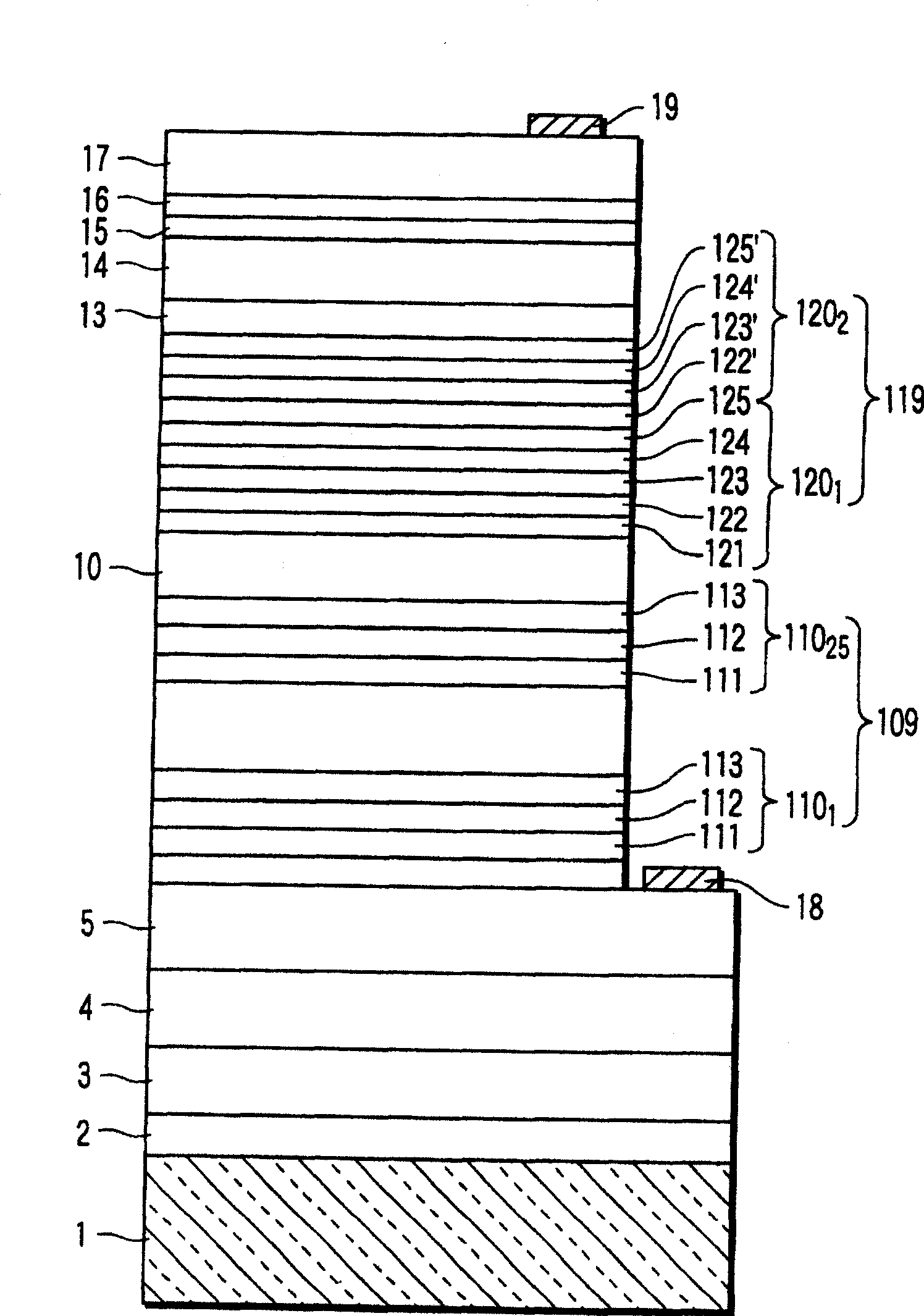
[0050] Figure 4 is a sectional view showing the structure of a light emitting device according to a second embodiment of the present invention. Like reference numerals denote equivalents to figure 1 parts of those parts. As shown in the figure, the light emitting device according to the present embodiment is obtained by combining the fluorescent substance with the light emitting device according to the first embodiment figure 1 The light-emitting diodes shown in combine the obtained white LEDs. That is, if Figure 4 As shown in , the reflective film 32 is provided on the inner surface of the package 31 formed of ceramics or the like, and the reflective film 32 is separately provided on the inner side surface and the bottom surface of the package 31 . The reflective film 32 is formed of, for example, aluminum. Will figure 1 The light emitting diode shown in is mounted on a reflective film 32 provided on the bottom surface of the package 31 .
[0051] The n-side electrod...
no. 3 example
[0061] Figure 5 is a sectional view showing the structure of a light emitting device according to a third embodiment of the present invention. Like reference numerals denote equivalents to figure 1 and 4 parts of those parts. Such as Figure 5 As shown in , the light-emitting device according to this embodiment is also made by combining the fluorescent substance with the light-emitting device according to the first embodiment figure 1 The light-emitting diodes shown in combine the obtained white LEDs. The difference from the second embodiment is that the fluorescent substance area is also disposed under the light emitting diodes.
[0062] Such as Figure 5 As shown in , a fluorescent substance region 41 containing blue, green or yellow fluorescent substances is formed on the reflective film 32 on the bottom surface of the package 31, and mounted and fixed on the fluorescent substance region 41figure 1 LEDs shown in . Bonding with an adhesive, welding, or the like may b...
PUM
 Abstract
Description
Claims
Application Information
 - R&D
- Intellectual Property
- Life Sciences
- Materials
- Tech Scout
- Unparalleled Data Quality
- Higher Quality Content
- 60% Fewer Hallucinations
Browse by: Latest US Patents, China's latest patents, Technical Efficacy Thesaurus, Application Domain, Technology Topic, Popular Technical Reports.
© 2025 PatSnap. All rights reserved.Legal|Privacy policy|Modern Slavery Act Transparency Statement|Sitemap|About US| Contact US: help@patsnap.com