Minisize photography module and substrates thereof

A substrate and miniature technology, applied in the direction of TV, color TV, electrical components, etc., can solve the problems of image shift, unable to independently check the sensing area, etc., and achieve the effect of avoiding image shift

Inactive Publication Date: 2009-07-29
ADVANCED SEMICON ENG INC
View PDF4 Cites 0 Cited by
  • Summary
  • Abstract
  • Description
  • Claims
  • Application Information

AI Technical Summary

Problems solved by technology

In order to solve the problem of the image shift of the micro-camera module, and after the die bonding, it is impossible to independently check the position of the sensing area of ​​the sensor chip relative to the substrate

Method used


Image

  • Minisize photography module and substrates thereof
  • Minisize photography module and substrates thereof
  • Minisize photography module and substrates thereof

Examples


Embodiment Construction

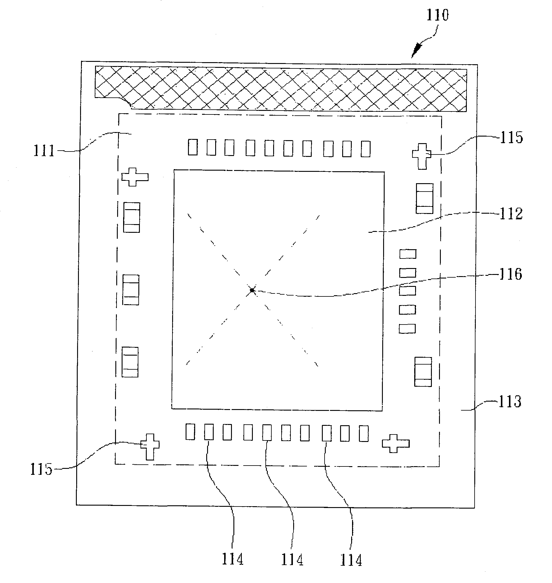
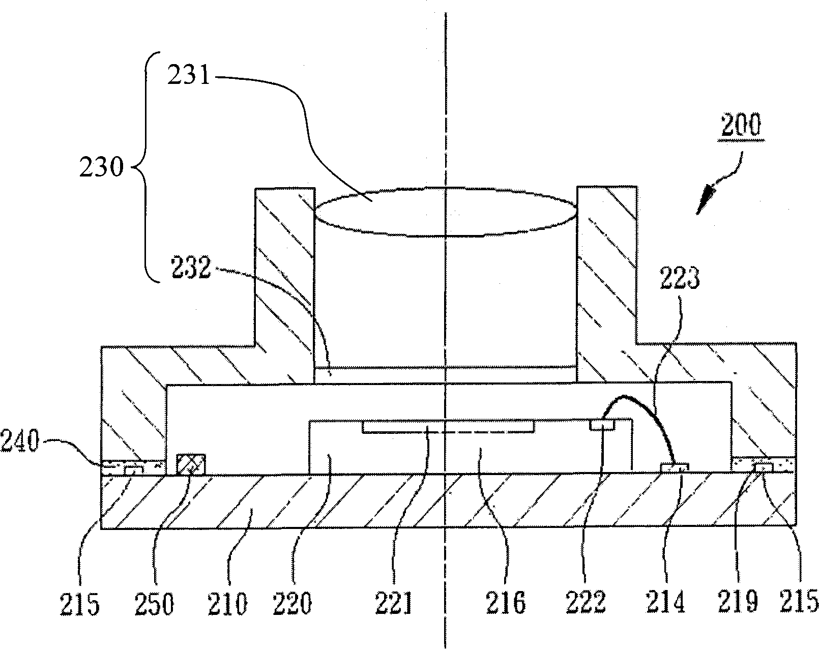
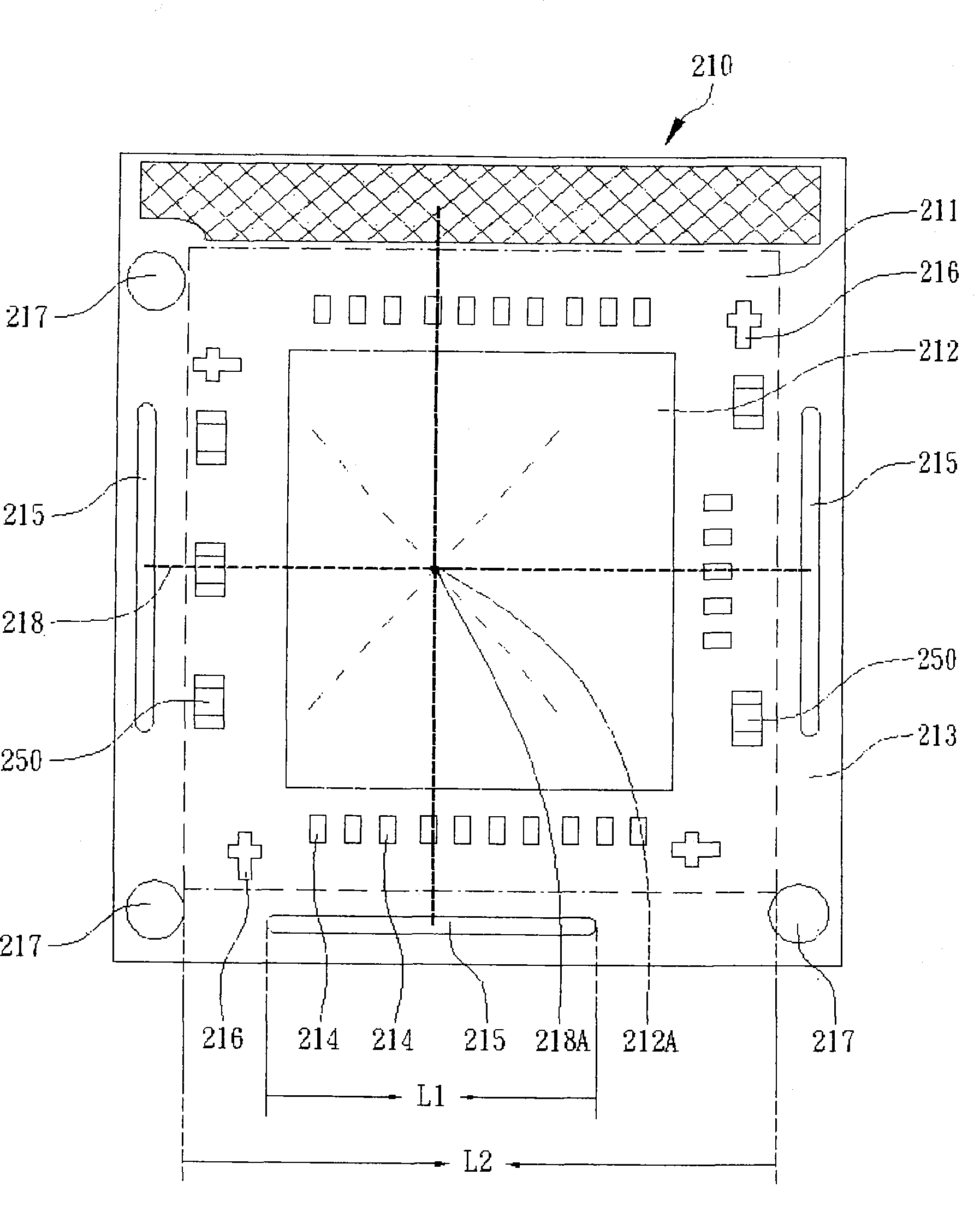
[0023] In a specific embodiment of the present invention, figure 2 is a schematic cross-sectional view of the micro-camera module, image 3 It is a schematic diagram of the upper surface of the substrate of a micro-camera module, Figure 4 is a schematic diagram of the upper surface of the substrate after die bonding.

[0024] Such as figure 2 As shown, the micro camera module 200 mainly includes a substrate 210, a sensor chip 220 and a lens module 230, the substrate 210 is used as a chip carrier, the sensor chip 220 and the lens module 230 are arranged on a surface 211 of the substrate 210 . In this embodiment, the sensor chip 220 can be a CMOS image sensor chip, which has a sensing region 221 that can accept an image and a plurality of bonding pads 222 . The lens module 230 is provided with a lens 231 and a filter 232 . In addition, a plurality of passive components 250 can be disposed on the surface 211 of the substrate 210 .

[0025] Such as image 3 As shown, the...


PUM


Abstract

The invention discloses a miniature camera module, comprising: a substrate, which has a surface, and the surface defines a die-bonding area and a module bonding area, the module bonding area surrounds the die-bonding area, and the substrate also It includes a plurality of connection pads and a plurality of detection strips located outside the die-bonding area; a sensor chip, which is attached to the die-bonding area, and the sensor chip has a sensing area, and the center of the sensing area is opposite to aligned at the intersection point of the vertical line of the test strip; and a lens module, which is combined to the module bonding area. The invention can ensure that the center of the sensing area is aligned with the intersection point of the vertical line of the detection strip after die bonding, so as to avoid the image deviation of the micro-camera module. After die bonding, the position of the sensing area of ​​the sensor chip relative to the substrate can be checked autonomously.

Description

technical field [0001] The invention relates to a miniature camera module (compact camera module, CCM), in particular to a miniature camera module capable of autonomous inspection after die bonding. Background technique [0002] A compact camera module (CCM) is a small image capture device, which can be applied to small cameras, digital cameras, or built into electronic products such as mobile phones, notebook computers, and palmtop computers. The main structure includes an image-receiving sensor chip on a substrate and a lens module with a lens in a barrel. The image is projected to a sensing area of ​​the sensor chip through the lens to convert the image into a storable electronic file. Therefore, the design requires that the center of the sensing area of ​​the sensor chip and the center of the lens module must be on the same straight line. Otherwise, the received image will show deviation. [0003] In the substrate (or chip carrier) structure of the existing micro-camer...

Claims


Application Information

Patent Timeline
Patent Type & Authority Patents(China)
IPC IPC(8): H01L27/146H01L23/498H01L23/544H04N5/225
Inventor 郑明政陈国华
Owner ADVANCED SEMICON ENG INC
Why Eureka
Try Eureka