Ion implantation system and method

An ion implantation system and ion implantation technology, which are applied in the field of ion implantation systems, can solve problems such as difficulty in applying ion implantation to larger-sized wafer workpieces, and achieve the effects of improving dose uniformity, saving costs, and improving production efficiency

CN102201321BActive Publication Date: 2013-04-10KINGSTONE SEMICONDUCTOR LIMITED COMPANY
1 Cites 0 Cited by

Patent Information

Authority / Receiving Office
CN · China
Patent Type
Patents(China)
Current Assignee / Owner
Publication Date
2013-04-10

Smart Images

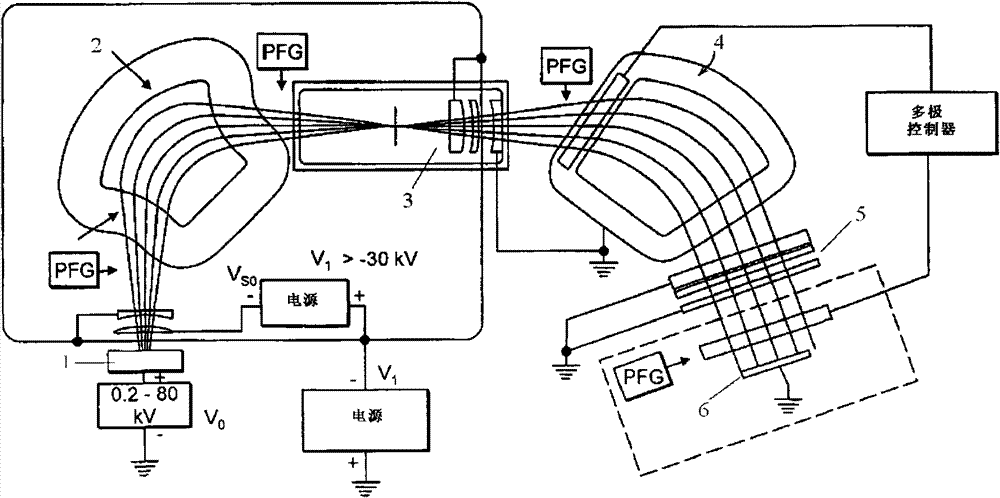
  • Figure 1
    Figure 1
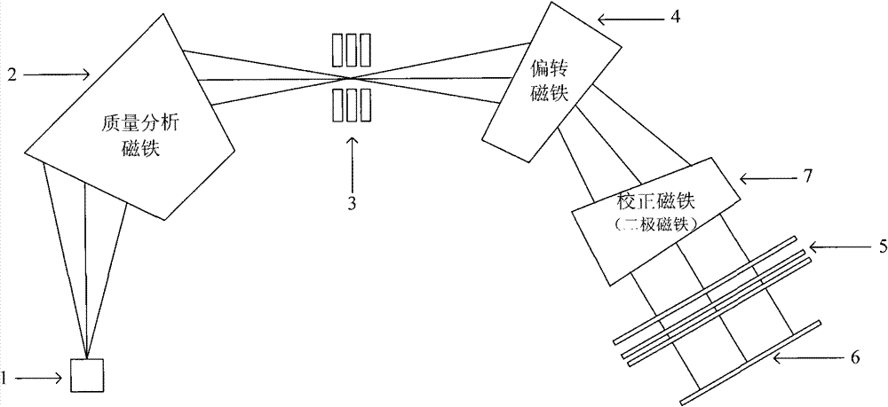
  • Figure 2
    Figure 2
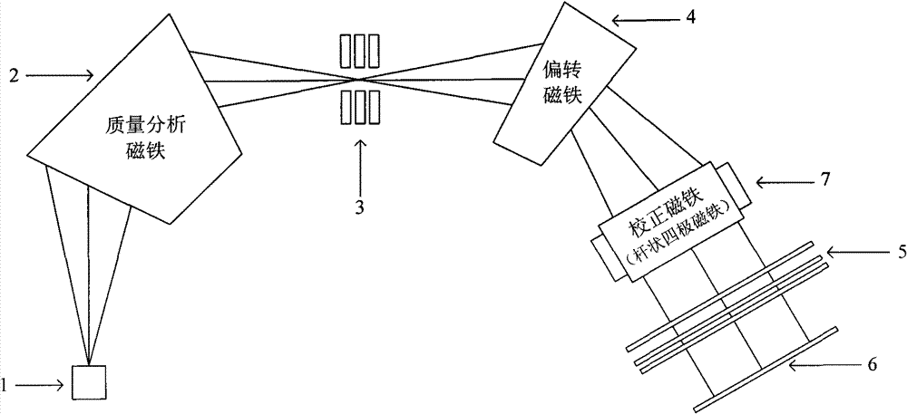
  • Figure 3
    Figure 3
Patent Text Reader

Abstract

The invention discloses an ion implantation system comprising an ion source and an extractor, a quality analysis magnet, a first acceleration-deceleration device, a deflecting magnet, a second acceleration-deceleration device and a work piece scanner. The deflecting magnet makes ion beams within a preset charge-to-mass ratio range divergent; the system further comprises a correction magnet arranged between the deflecting magnet and the second acceleration-deceleration device, and the correction magnet is used for correcting the ion beam deflected and diverged by the deflecting magnet within the preset charge-to-mass ratio range to be a preset implantation angle. The invention further discloses an ion implantation method realized by utilizing the ion implantation system. Through the ion implantation system and method, disclosed by the invention, the evenness of dosage of ions implanted into a large wafer work piece can be improved, thus the production efficiency is improved, and the cost consumed due to the comprehensive update of the whole ion implantation system can be largely saved.
Need to check novelty before this filing date? Find Prior Art

Description

technical field

[0001] The invention relates to the field of semiconductor manufacturing, in particular to an ion implantation system and method. Background technique

[0002] The ion implantation process is used to introduce atoms or molecules, usually called impurities, into the target substrate, thereby changing the physical and chemical properties of the substrate material. Of particular interest is the use of ion implantation to dope single or polycrystalline silicon, a routine process for the manufacture of modern integrated circuits. As the production of semiconductor products has gradually moved towards larger wafers (from 8 inches to 12 inches, and is now developing to 18 inches), the single wafer process (processing one wafer at a time) has recently been widely adopted. However, the larger the wafer workpiece, the longer it takes to implant, and at the same time, it becomes more and more difficult to achieve a certain implant dose uniformity and implant angle unif...

Examples

Embodiment Construction

[0024] The preferred embodiments of the present invention are given below in conjunction with the accompanying drawings to describe the technical solution of the present invention in detail.

[0025] Such as figure 2 and image 3 As shown, similar to the existing system, the ion implantation system of the present invention includes an ion source and an extraction device 1 for extracting an ion beam from the ion source. On the transmission path of the ion beam, the ion implantation system of the present invention is also sequentially provided with: a mass analysis magnet 2, which is used to deflect the beam current by about 90°, so as to select the ion beam within a preset charge-to-mass ratio range. In addition, a group of small magnetic poles driven by a motor can also be preferably set in the mass analysis magnet 2, and by adjusting the position of the group of small magnetic poles, the beam current passing through the mass analysis magnet 2 can be controlled. Fine-tuning...