Array substrate, display device and driving method of display device

An array substrate and display device technology, which is applied in static indicators, nonlinear optics, instruments, etc., can solve the problems of inability to guarantee the charging time of pixel electrodes and insufficient response time of liquid crystal display panels, etc., and achieve long screen response time and guaranteed screen The effect of quality, long charging time

Inactive Publication Date: 2012-10-03
BOE TECH GRP CO LTD +1
View PDF5 Cites 58 Cited by
  • Summary
  • Abstract
  • Description
  • Claims
  • Application Information

AI Technical Summary

Problems solved by technology

[0006] The embodiment of the present invention provides an array substrate, a display device and a driving method of the display device, which are used to solve the problem that the existing liquid crystal display panel cannot guarantee the charging time of the pixel electrodes and the response time of the liquid crystal display panel is insufficient while increasing the refresh frequency. The problem

Method used


Image

  • Array substrate, display device and driving method of display device
  • Array substrate, display device and driving method of display device
  • Array substrate, display device and driving method of display device

Examples


Embodiment Construction

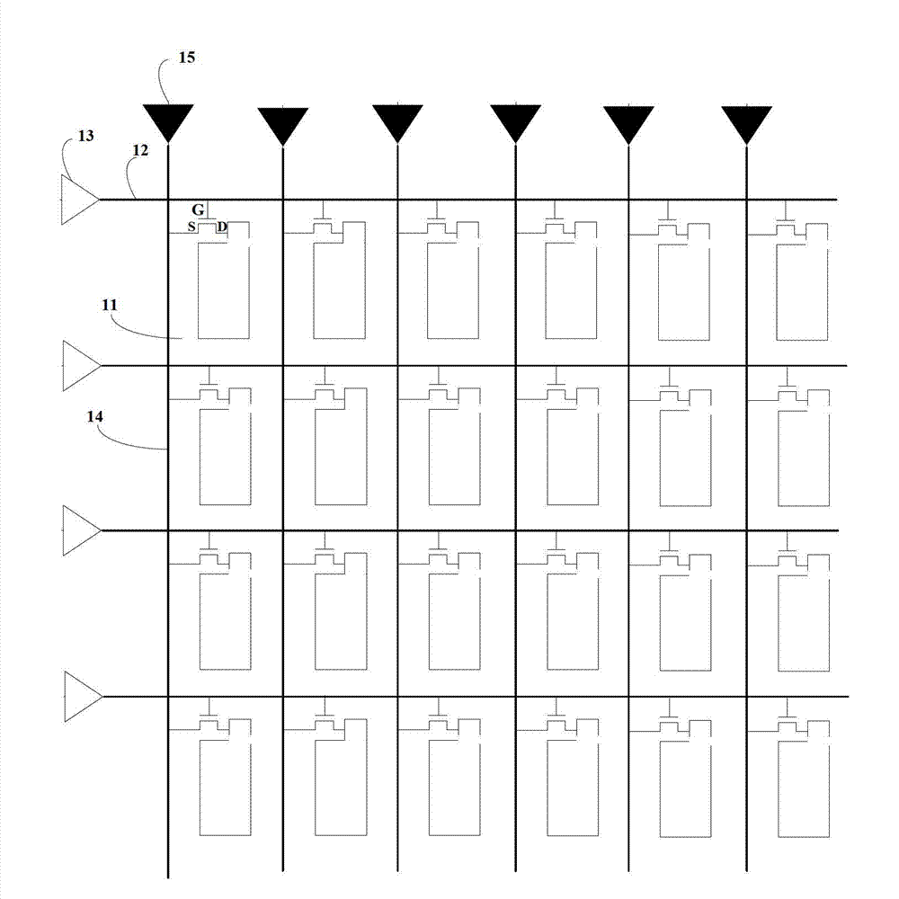
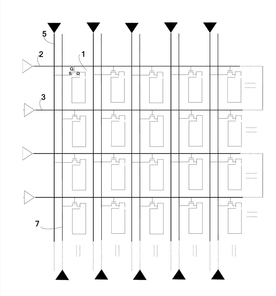
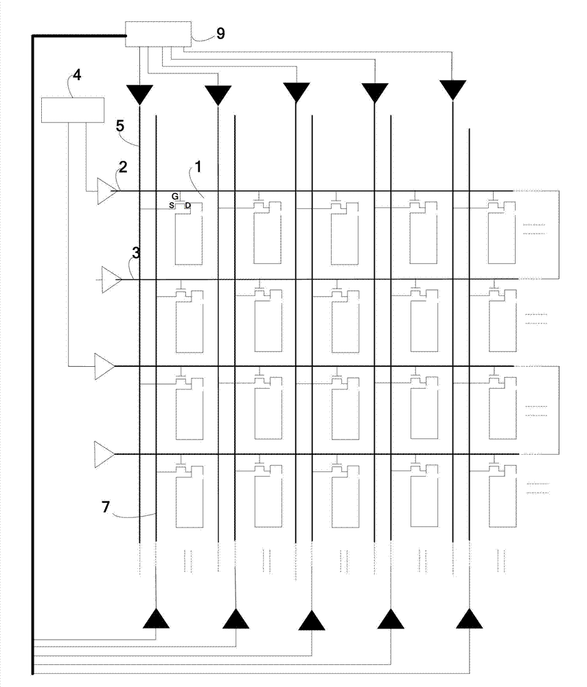
[0032] In order to make the technical problems, technical solutions and advantages to be solved by the embodiments of the present invention clearer, the following will describe in detail with reference to the drawings and specific embodiments.

[0033] like figure 2 As shown, the embodiment of the present invention provides an array substrate, including:

[0034] Substrate;

[0035] A plurality of pixel units 1 formed on the substrate in matrix form, wherein each pixel unit 1 includes a thin film transistor and a pixel unit connected to the drain D of the thin film transistor;

[0036] The above-mentioned array substrate may also include:

[0037] Gate lines, each row of pixel units corresponds to a gate line, and each gate line is connected to the gate G of the thin film transistor in the corresponding pixel unit, and the gate line 2 corresponding to the 2mth row of pixel units corresponds to the gate line 2 corresponding to the 2mth row - Gate lines 3 of pixel units in o...


PUM


Abstract

The invention provides an array substrate, a display device and a driving method of the display device, so as to solve the problems that the refresh rate of the charging time of a pixel electrode can not be ensured as the existing liquid crystal display panel is improved at the same time, and the response time of the liquid crystal display panel is insufficient. The array substrate comprises a substrate, gate lines and data lines, wherein the gate lines corresponding to the 2m-th row of pixel units and the gate lines corresponding to the (2m-1)th row of the pixel units receive the same control signal; and each column of the pixel units corresponds to two data lines and the two data lines comprise a first data line and a second data line. By utilizing the technical scheme, the refresh rate of the display device can be improved, and a pixel electrode can be guaranteed to have sufficiently long charging time at the same time, thus the response time of a picture of the display device is sufficiently long and the quality of the picture is ensured.

Description

technical field [0001] The invention relates to the technical field of liquid crystal display panels, in particular to an array substrate, a display device and a driving method for the display device. Background technique [0002] An existing thin film transistor liquid crystal display panel (TFT-LCD) includes an array substrate, a color filter substrate, and a liquid crystal layer arranged between the array substrate and the color filter substrate. [0003] like figure 1 As shown, the array substrate includes: a substrate; a plurality of pixel units 11 formed on the substrate in a matrix, wherein each pixel unit 11 includes a thin film transistor and a pixel electrode connected to the drain D of the thin film transistor; a gate line 12, It is connected with the gate G of the thin film transistor in a row of pixel units; the gate driver 13 is used to provide the gate signal to the gate line 12; the data line 14 is connected with the source S of the thin film transistor in a...

Claims


Application Information

Patent Timeline
Patent Type & Authority Applications(China)
IPC IPC(8): G02F1/1362G02F1/1368G02F1/133G09G3/36
CPCG02F1/1368G02F1/1362G09G3/3648G02F1/136286G09G3/36G09G2310/0205G02F1/133
Inventor 肖利军
Owner BOE TECH GRP CO LTD
Why Eureka
Try Eureka