

Reduce ocd measurement noise with metal via slots
A metal through hole and through hole slot technology, which is used in semiconductor/solid-state device testing/measurement, electrical components, electrical solid-state devices, etc.
- Summary
- Abstract
- Description
- Claims
- Application Information
AI Technical Summary
Problems solved by technology
Method used
Image

Examples
Embodiment Construction
[0030] It is understood that the following disclosure provides many different embodiments, or examples, for implementing various elements of the invention. Specific examples of components and arrangements are described below to simplify the present disclosure. These are of course merely examples and are not intended to be limiting. In addition, the present invention may repeat reference numerals and / or letters in each example. This repetition is for simplicity and clarity and does not in itself indicate a relationship between the various embodiments and / or structures discussed.
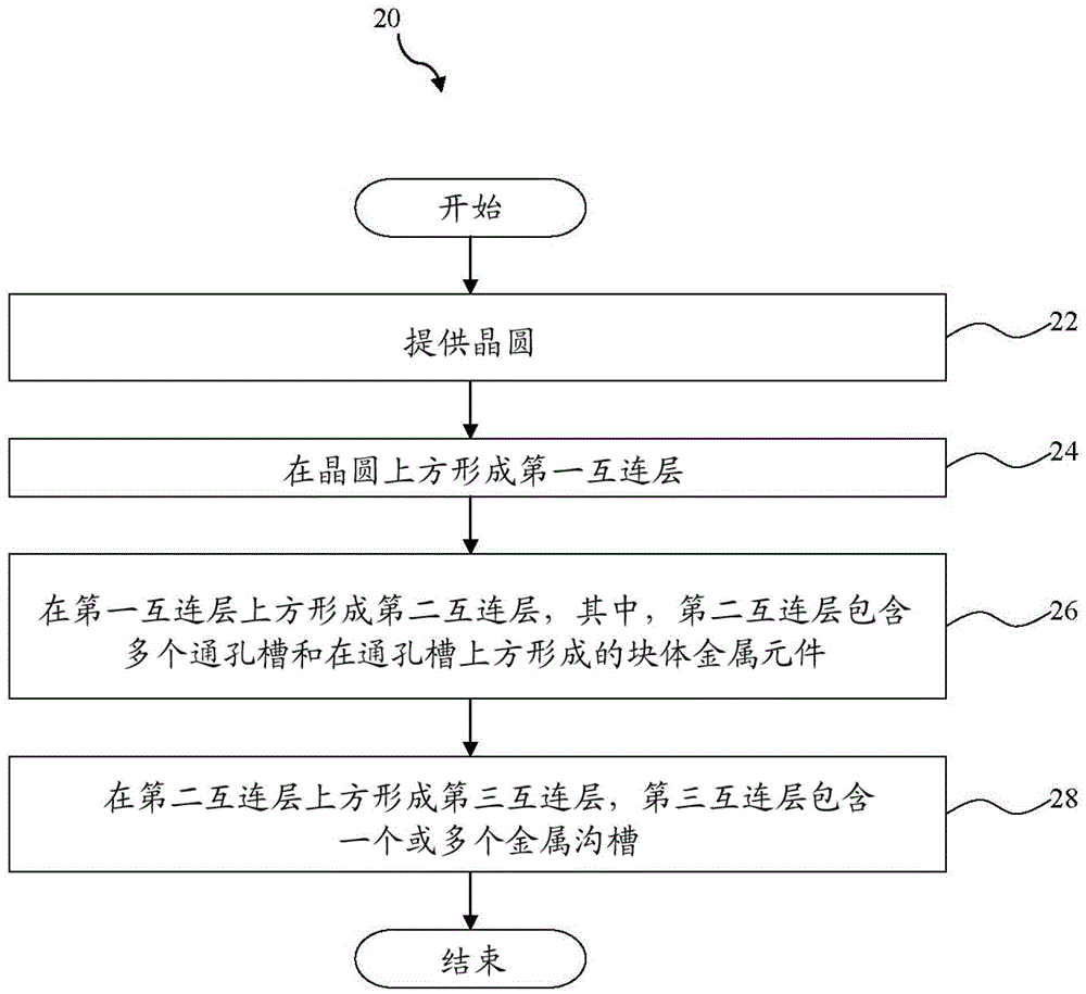
[0031] figure 1 is a flowchart of a method 20 for fabricating a semiconductor device. Method 20 includes block 22, wherein a wafer is provided. A horizontal surface of the wafer on which the interconnect structure is formed is defined by a first horizontal direction and a second horizontal direction. Method 20 includes block 24 wherein a first interconnect layer of an interconnect structure is fo...
PUM
 Abstract
Description
Claims
Application Information