Array substrate and display device

A technology of array substrate and display area, applied in optics, instruments, electrical components, etc., can solve the problems of large difference in characteristics and low detection accuracy, and achieve the effect of improving accuracy

Inactive Publication Date: 2014-10-08
BOE TECH GRP CO LTD +1
View PDF6 Cites 8 Cited by
  • Summary
  • Abstract
  • Description
  • Claims
  • Application Information

AI Technical Summary

Problems solved by technology

[0006] Embodiments of the present invention provide an array substrate and a display device, which are used to solve the problem of low detection accuracy in the prior art due to the large difference in characteristics between the thin film transistors in the detection area and the thin film transistors in the display area.

Method used


Image

  • Array substrate and display device
  • Array substrate and display device
  • Array substrate and display device

Examples


Embodiment Construction

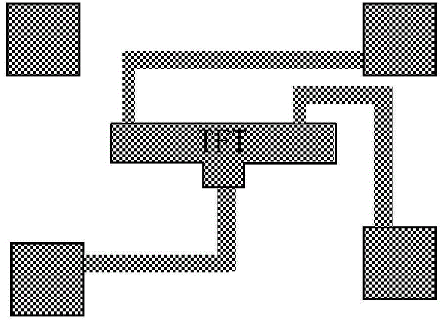
[0026] Embodiments of the present invention provide a probe device and a detection device, which are used to solve the problem in the prior art that a test signal cannot be loaded into an array substrate due to the position limitation of a probe body.

[0027] The following will clearly and completely describe the technical solutions in the embodiments of the present invention with reference to the accompanying drawings in the embodiments of the present invention. Obviously, the described embodiments are only some, not all, embodiments of the present invention. Based on the embodiments of the present invention, all other embodiments obtained by persons of ordinary skill in the art without making creative efforts belong to the protection scope of the present invention.

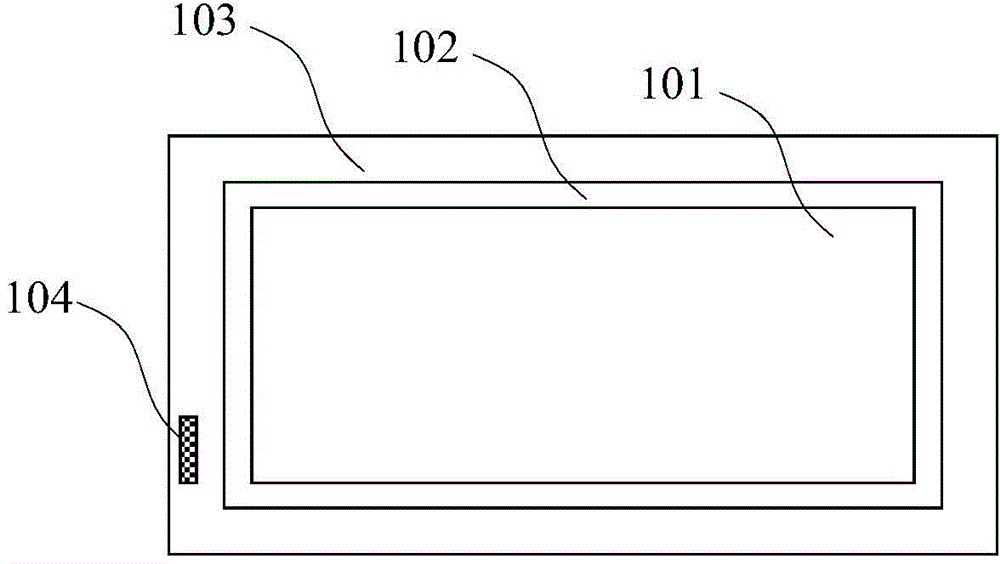
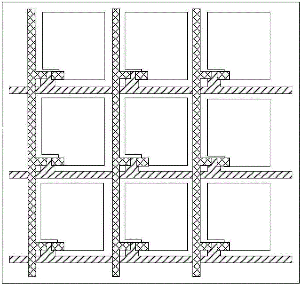
[0028] Embodiment 1 of the present invention provides an array substrate, including a display area and a dummy pixel area located on the periphery of the display area, and a second pixel unit is arranged in the ...


PUM


Abstract

The invention provides an array substrate and a display device. The array substrate and the display device are used for solving the problem that due to the fact that the difference between the feature of a thin film transistor in a detection area and the feature of a thin film transistor in a display area is large, the detection accuracy is low. The array substrate comprises a display area and a pseudo pixel area located on the periphery of the display area. A second pixel unit is arranged in the pseudo pixel area which comprises at least one detection unit. Each detection unit comprises a second pixel unit. Each second pixel unit is correspondingly provided with one thin film transistor. All electrodes of all the thin film transistors are respectively connected with external testing equipment through testing wires.

Description

technical field [0001] The present invention relates to the technical field of display devices, in particular to an array substrate and a display device. Background technique [0002] The array process is a stage in the manufacturing process of a Thin Film Transistor Liquid Crystal Display (TFT-LCD) device. In the array process, it is necessary to form a thin film transistor array circuit on a glass substrate. The quality of the array circuit directly determines the quality of the thin film transistor liquid crystal display, and the detection of the array circuit has become an important process in the manufacturing process. [0003] Such as figure 1 As shown, the array substrate 100 includes: a display area 101 , a routing area 102 and a peripheral area 103 in the early stage of fabrication. The display area 101 includes a plurality of first pixel units for display formed by staggered gate lines and data lines, and each of the first pixel units corresponds to a thin film ...

Claims


Application Information

Patent Timeline
Patent Type & Authority Applications(China)
IPC IPC(8): G02F1/13
CPCG02F1/1368G02F1/136254H01L22/32H01L22/34
Inventor 高玉杰朴相镇
Owner BOE TECH GRP CO LTD
Why Eureka
Try Eureka