
Shell and preparation method thereof
A shell and substrate technology, applied in the field of shell and its preparation, can solve the problem of not being able to present a three-dimensional effect, etc., and achieve the effect of avoiding pattern fading or film layer shedding and high pattern precision.
- Summary
- Abstract
- Description
- Claims
- Application Information
AI Technical Summary
Problems solved by technology
Method used
Image

Examples
Embodiment Construction
[0070] In order to make the object, technical solution and advantages of the present invention clearer, the implementation manner of the present invention will be further described in detail below in conjunction with the accompanying drawings.
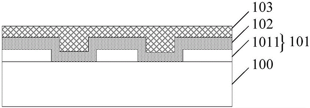
[0071] figure 1 is a structural schematic diagram of a housing provided by an embodiment of the present invention, the housing is suitable for electronic equipment, see figure 1 , the shell consists of:
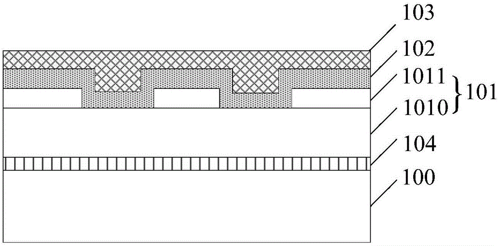
[0072] The transparent substrate 100 and the micro-nano structure layer 101 covered on the transparent substrate 100, the micro-nano structure layer 101 is arranged on the side of the transparent substrate 100 close to the electronic components in the electronic device, the micro-nano structure layer 101 includes micro-nano scale grooves and Micro-nano pattern composed of bosses.
[0073] In an embodiment of the present invention, the housing includes a transparent substrate and a micro-nano structure layer covering the transparent ...
PUM
| Property | Measurement | Unit |
|---|---|---|
| thickness | aaaaa | aaaaa |
Abstract
Description
Claims
Application Information