Fan-out packaging device and packaging method thereof

A packaging method and a technology for packaging devices, which are applied in the fields of electric solid-state devices, semiconductor devices, semiconductor/solid-state device manufacturing, etc., can solve the problems of complex wiring process and small number of packaged chips, and achieve simple wiring process, improve packaging efficiency, increase Quantity effect

Active Publication Date: 2017-05-31
NANTONG FUJITSU MICROELECTRONICS
View PDF7 Cites 1 Cited by
  • Summary
  • Abstract
  • Description
  • Claims
  • Application Information

AI Technical Summary

Problems solved by technology

[0004] Embodiments of the present invention provide a fan-out packaging device and a packaging method thereof, so as to solve the technical problems in the prior art that the number of chips packaged in a fan-out panel is small and the wiring process is complicated

Method used


Image

  • Fan-out packaging device and packaging method thereof
  • Fan-out packaging device and packaging method thereof
  • Fan-out packaging device and packaging method thereof

Examples


Embodiment Construction

[0054] The present invention will be described in further detail below in conjunction with the accompanying drawings and embodiments. In particular, the following examples are only used to illustrate the present invention, but not to limit the scope of the present invention. Similarly, the following embodiments are only some of the embodiments of the present invention rather than all embodiments, and all other embodiments obtained by those skilled in the art without creative efforts fall within the protection scope of the present invention.

[0055] see figure 1 , figure 1 It is a schematic flowchart of a preferred embodiment of the fan-out structure packaging method of the present invention, and the packaging method includes but not limited to the following steps.

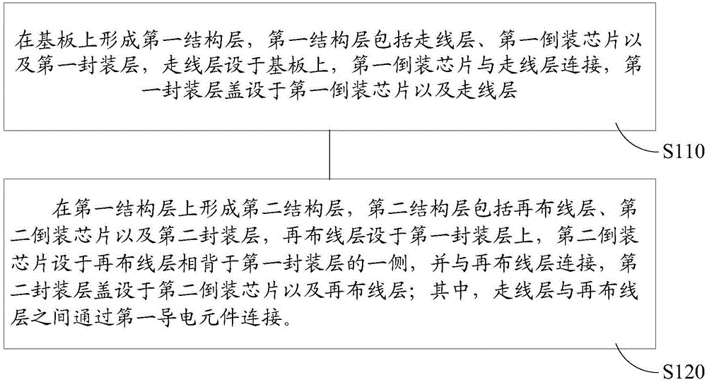
[0056] Step S110, forming a first structure layer on the substrate.

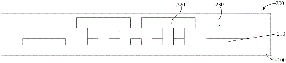
[0057] see figure 2 , figure 2 is a structural schematic diagram after forming the first structural layer on the substrate. Wherein, th...


PUM


Abstract

The invention provides a fan-out packaging device and a packaging method thereof. The method comprises the steps of forming a first structure layer on a substrate, wherein the first structure layer is composed of a wiring layer, a first flip chip and a first packaging layer; a second structure layer is composed of a re-wiring layer, a second flip chip and a second packaging layer, the re-wiring layer is arranged on the first packaging layer, and the second flip chip is arranged on one side of the re-wiring layer, which backs to the first packaging layer, and connected with the re-wiring layer, the second packaging layer covers the second flip chip and the re-wiring layer; the wiring layer and the re-wiring layer are connected through a first conducting element. Compared with the prior art, the fan-out packaging device and the packaging method thereof can increase the number of embedded chip by embedding the chips into the layers of a fan-out panel, and meanwhile, are simple in wiring processes, capable of communicating chips on different layers and saving the processes of barrier removal, plastic package and the like, thereby improving the packaging efficiency of fan-out devices.

Description

technical field [0001] The invention relates to the technical field of semiconductors, in particular to a fan-out packaging device and a packaging method thereof. Background technique [0002] In the field of semiconductors, fan-out packaging is a very important process. In the fan-out (fan-out) packaging process, there can be additional functions for the PCB board, and it can also provide convenience for connection, and during work These devices can also be protected, so it is necessary to provide a packaging structure for embedding devices in a circuit board, and these packaged devices are placed on a printed circuit board (PCB) together with other devices. PCBs with the above devices are used in products such as computers or cellular phones. With the desire to reduce the size of products such as computers and cellular phones, there is a need to reduce the size of PCBs and packaged devices without sacrificing functionality. [0003] System-in-Package refers to having mul...

Claims


Application Information

Patent Timeline
Patent Type & Authority Applications(China)
IPC IPC(8): H01L21/48H01L21/50H01L21/60H01L23/498H01L25/00
CPCH01L21/4846H01L21/50H01L23/49816H01L24/81H01L25/00H01L2224/0231H01L2224/0233
Inventor 沈海军
Owner NANTONG FUJITSU MICROELECTRONICS
Why Eureka
Try Eureka