Three-dimensional memory and manufacturing method thereof

A manufacturing method and memory technology, applied in the direction of electric solid-state devices, semiconductor devices, electrical components, etc., can solve problems such as storage failure of three-dimensional memory, achieve the effects of ensuring storage performance, improving storage performance, and avoiding failure

Pending Publication Date: 2018-09-04
YANGTZE MEMORY TECH CO LTD
View PDF9 Cites 24 Cited by
  • Summary
  • Abstract
  • Description
  • Claims
  • Application Information

AI Technical Summary

Problems solved by technology

[0005] The invention provides a three-dimensional memory and its manufacturing method, which is used to solve the problem that the existing three-dimensional memory is prone to storage failure, so as to improve the storage performance of the three-dimensional memory

Method used


Image

  • Three-dimensional memory and manufacturing method thereof
  • Three-dimensional memory and manufacturing method thereof
  • Three-dimensional memory and manufacturing method thereof

Examples


Embodiment Construction

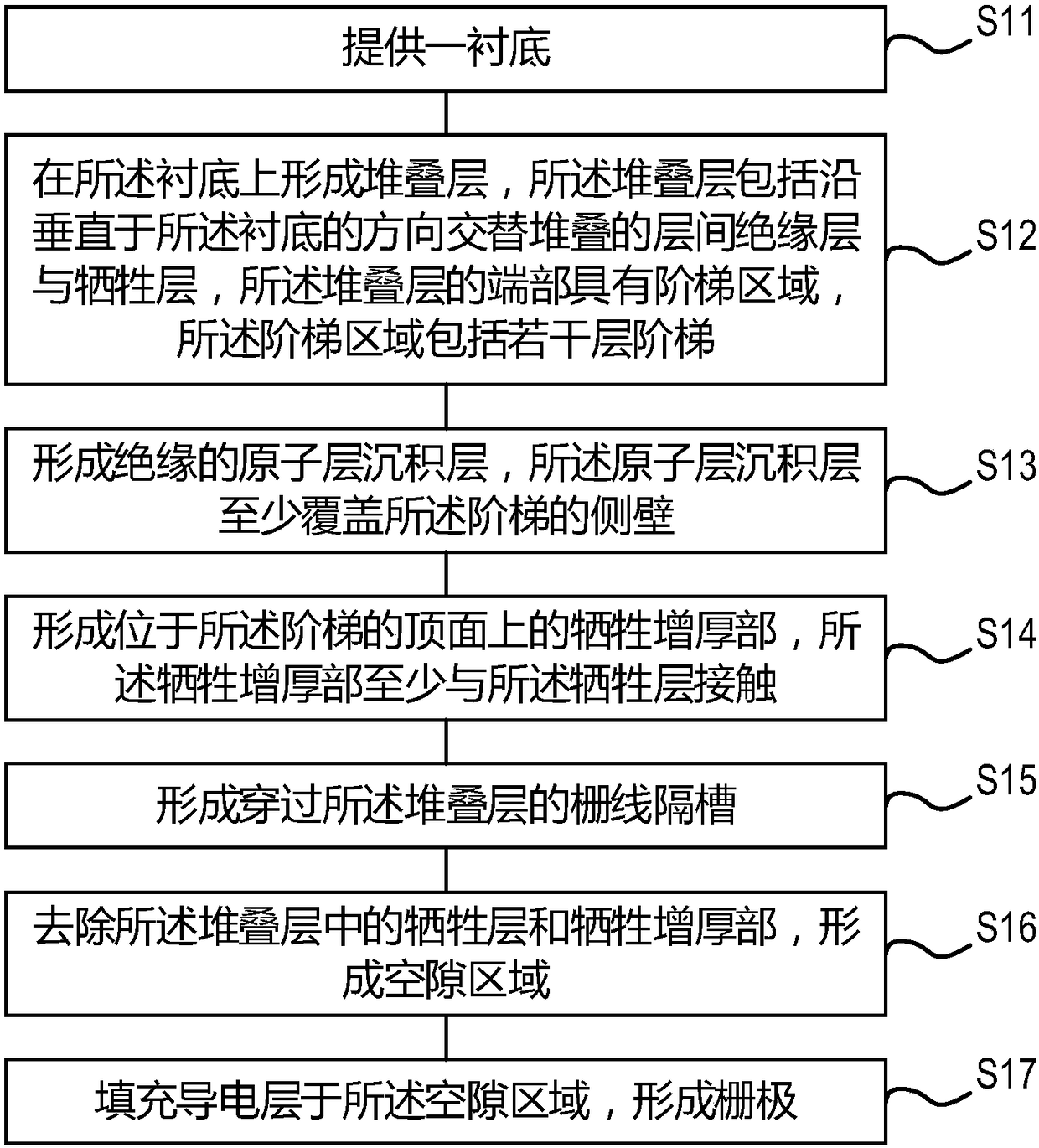
[0049] The specific implementation of the three-dimensional memory and its manufacturing method provided by the present invention will be described in detail below in conjunction with the accompanying drawings.

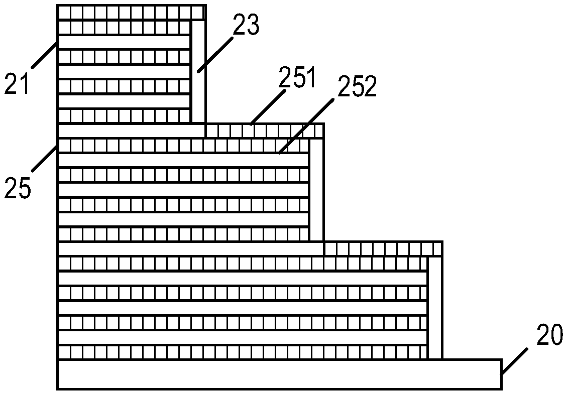
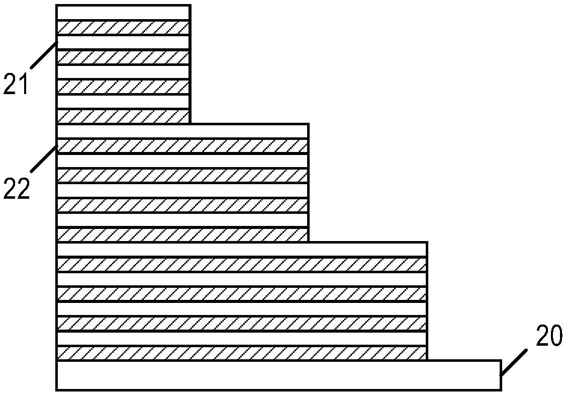
[0050] The three-dimensional memory has a stacked structure, and the stacked structure includes several layers of alternately arranged gate electrodes and interlayer insulating layers. The stack structure includes a core area and a step area arranged around the core area, the core area is used for data storage, the step area is used for connecting with one end of the metal plug, and the other end of the metal plug is used for Connect with the interconnect structure. In the process of etching the gate located in the stepped area to form a plug via hole, it is very easy to break down the gate layer, which will cause the gate of the adjacent layer to appear after the via hole is filled with metal to form a plug. Short circuit causes the control failure of the storage un...


PUM


Abstract

The invention relates to the technical field of semiconductor manufacturing and particularly relates to a three-dimensional memory and a manufacturing method thereof. The three-dimensional memory comprises a substrate, a stacking structure and an insulated atom layer settling layer, wherein the stacking structure is formed on the substrate and comprises grid electrodes, interlayer insulating layers and multiple layers of steps, the grid electrodes and the interlayer insulating layers are alternately stacked along the direction vertical to the substrate, and the steps are located at the end part of the substrate; the grid electrodes comprise thickened parts, and the thickened parts protrude along the direction, towards the stacking structure, of the substrate and are located on the top surfaces of the steps; and the insulated atom layer settling layer is in contact with the side walls of the steps and is used for electrically isolating the grid electrode between two layers of the steps.According to the three-dimensional memory, the problem that a three-dimensional memory easily malfunctions is avoided, and the memory performance of the three-dimensional memory is improved.

Description

technical field [0001] The invention relates to the technical field of semiconductor manufacturing, in particular to a three-dimensional memory and a manufacturing method thereof. Background technique [0002] As technology develops, the semiconductor industry is constantly seeking new ways to produce a greater number of memory cells per memory die in a memory device. In non-volatile memory, such as NAND memory, one way to increase the memory density is by using vertical memory arrays, that is, 3D NAND (three-dimensional NAND) memory; 32 layers developed to 64 layers, or even higher layers. [0003] Generally, a three-dimensional memory includes a stack structure formed by alternately stacking gates and insulating layers, and a plug (Contact) is electrically connected to the gate at a step region of the stack structure. However, in the actual manufacturing process of the three-dimensional memory, in order to achieve a good electrical connection between the plug and the gat...

Claims


Application Information

Patent Timeline
Patent Type & Authority Applications(China)
IPC IPC(8): H01L27/11551H01L27/11578H01L29/423H01L21/28
CPCH01L29/40114H01L29/40117H01L29/42324H01L29/4234H10B41/20H10B43/20
Inventor 李思晢华文宇肖莉红赵祥辉张帜张富山
Owner YANGTZE MEMORY TECH CO LTD
Why Eureka
Try Eureka