Electronic device housing, and electronic device and housing manufacturing technology

A technology of electronic devices and manufacturing processes, applied in lamination devices, telephone communications, electrical components, etc., can solve the problems of general anti-fingerprint effect, discomfort of human eyes, fingerprints easy to stay on the glass surface, etc., so as to solve the problem of glare and enhance The effect of anti-fingerprint function, strong texture and business sense

Active Publication Date: 2018-11-02
GUANGDONG OPPO MOBILE TELECOMM CORP LTD
View PDF4 Cites 37 Cited by
  • Summary
  • Abstract
  • Description
  • Claims
  • Application Information

AI Technical Summary

Problems solved by technology

[0003] However, the shells of electronic devices made of glass in the related art also have certain application defects.
For example, due to the glare problem that causes discomfort to the human eye, the anti-fingerprint effect achieved by directly coating the glare surface of the glass substrate with an anti-fingerprint film layer is average, and fingerprints are easy to stay on the glass surface

Method used


Image

  • Electronic device housing, and electronic device and housing manufacturing technology
  • Electronic device housing, and electronic device and housing manufacturing technology
  • Electronic device housing, and electronic device and housing manufacturing technology

Examples


Embodiment Construction

[0027] Embodiments of the present application are described in detail below, examples of which are shown in the drawings, wherein the same or similar reference numerals denote the same or similar elements or elements having the same or similar functions throughout. The embodiments described below by referring to the figures are exemplary, and are only for explaining the present application, and should not be construed as limiting the present application.

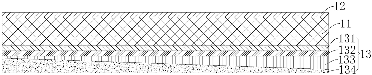
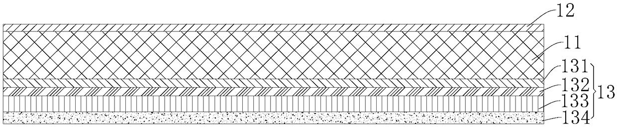
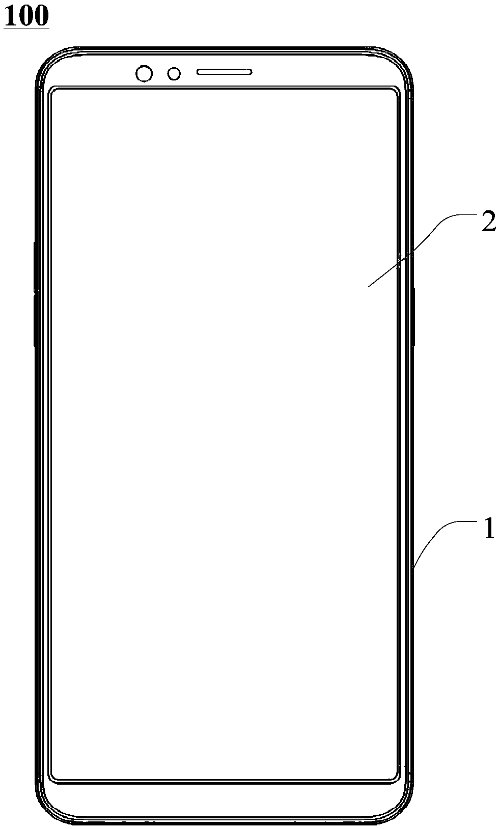
[0028] Refer below Figure 1-Figure 2 The housing 1 of the electronic device according to the embodiment of the present application is described.

[0029] like Figure 1-Figure 2 As shown, the housing 1 of the electronic device according to the embodiment of the first aspect of the present application includes: a glass substrate 11 , a color function layer 13 and an anti-fingerprint film layer 12 .

[0030] Specifically, the outer surface of the glass base 11 (the "outer surface of the glass base 11" refers to the surface ...


PUM

PropertyMeasurementUnit
thicknessaaaaaaaaaa

Abstract

The invention discloses an electronic device housing, and electronic device and housing manufacturing technology. The electronic device housing comprises a glass substrate, a color function layer, andan anti-fingerprint film layer; the external surface of the glass substrate is an anti-dazzle surface; the color function layer is arranged on the internal surface of the glass substrate; the anti-fingerprint film layer is arranged on the external surface of the glass substrate. According to the electronic device housing, the external surface of the glass substrate is designed to be an anti-dazzle surface, so that dazzling caused by glass housings is avoided, and at the same time, the external surface of the housing is provided with better qualitative sense and business sense; the anti-fingerprint film layer is adopted on the surface of the anti-dazzle surface, so that anti-fingerprint function is improved further; the color function layer is adopted, so that the anti-dazzle surface of the housing is provided with certain color with certain metal qualitative sense, and the qualitative sense and the sense of beauty of the electronic device housing are improved.

Description

technical field [0001] The present application relates to the field of electronic devices and their manufacture, and in particular to a casing of an electronic device, an electronic device and a manufacturing process of the casing. Background technique [0002] In recent years, the appearance of electronic devices such as mobile phones has attracted more and more attention. The outer shell of some electronic devices is made of glass, and the anti-fingerprint film is coated on the outer surface of the shell to achieve the effect of anti-fingerprint, and the color is coated on the glass substrate. The functional film allows the housing to have a rich variety of colors. [0003] However, the casing of the electronic device made of glass in the related art also has certain application defects. For example, due to the glare problem that causes discomfort to the human eye, the anti-fingerprint effect achieved by directly coating the glare surface of the glass substrate with an an...

Claims


Application Information

Patent Timeline
Patent Type & Authority Applications(China)
IPC IPC(8): B32B17/10B32B27/36B32B33/00B32B7/12B32B38/00B32B38/14B32B37/24C03C15/00C03C15/02C03C17/00H04M1/02
CPCB32B7/12B32B17/064B32B27/36B32B33/00B32B37/24B32B38/00B32B38/0004B32B38/145B32B2037/243C03C15/00C03C15/02C03C17/002H04M1/0283
Inventor 杨光明
Owner GUANGDONG OPPO MOBILE TELECOMM CORP LTD
Why Eureka
Try Eureka