UFS storage array system based on FPGA control and data transmission method

A storage array and data technology, applied in electrical digital data processing, general-purpose stored program computers, digital computer components, etc., can solve the problems of lack and inability to make full use of UFS chips, and achieve ultra-low power consumption, efficient defragmentation, The effect of reducing the difficulty of adaptation

Active Publication Date: 2019-07-30
SHANDONG INSPUR SCI RES INST CO LTD
View PDF6 Cites 5 Cited by
  • Summary
  • Abstract
  • Description
  • Claims
  • Application Information

AI Technical Summary

Problems solved by technology

[0003]Currently, there is a lack of high-speed storage devices with Thunderbolt 3 interface on the market, and it is impossible to make full use of the high-speed advantages of UFS chips and Thunderbolt 3 interface

Method used


Image

  • UFS storage array system based on FPGA control and data transmission method
  • UFS storage array system based on FPGA control and data transmission method
  • UFS storage array system based on FPGA control and data transmission method

Examples


Embodiment Construction

[0029] In order to enable those skilled in the art to better understand the solutions of the present invention, the present invention will be further described in detail below in conjunction with specific embodiments. Apparently, the described embodiments are only some of the embodiments of the present invention, not all of them. Based on the embodiments of the present invention, all other embodiments obtained by persons of ordinary skill in the art without making creative efforts fall within the protection scope of the present invention.

[0030] A preferred embodiment is given below:

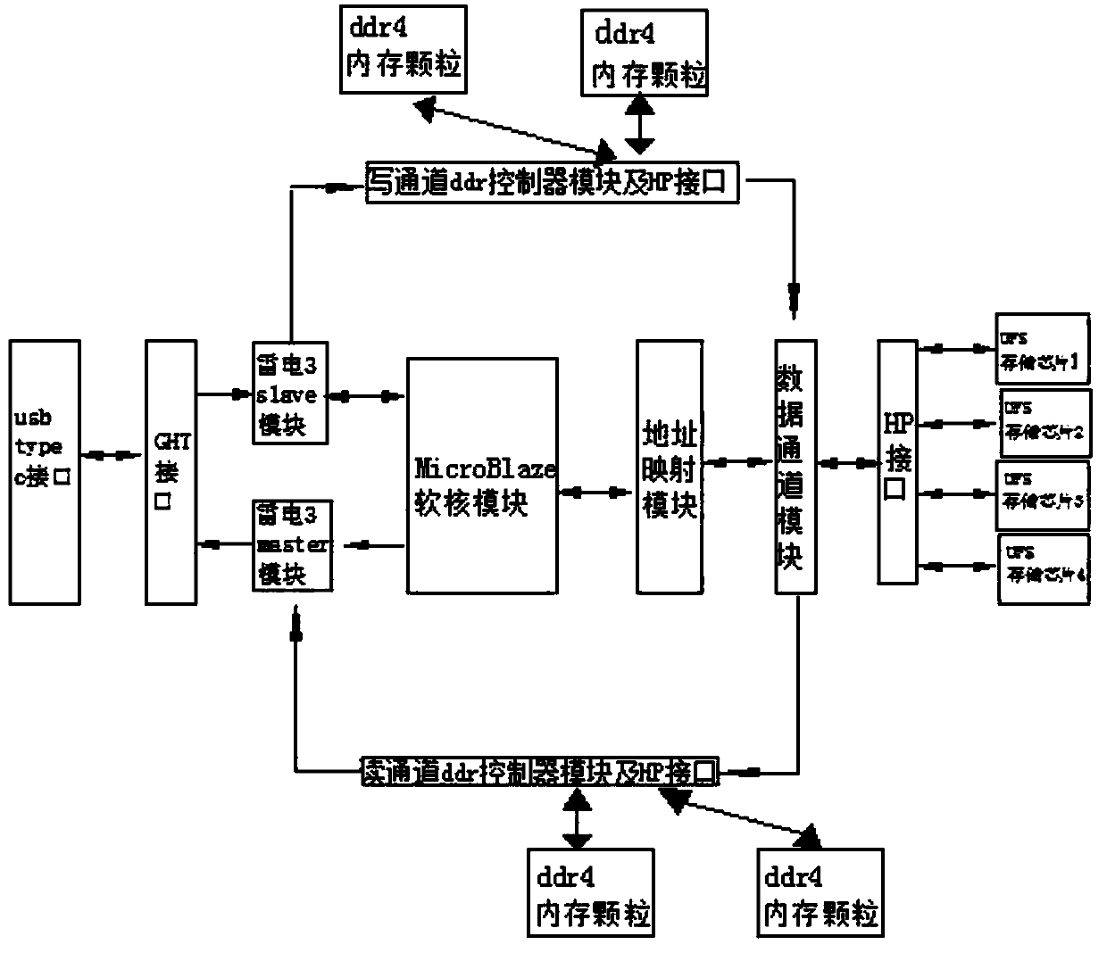
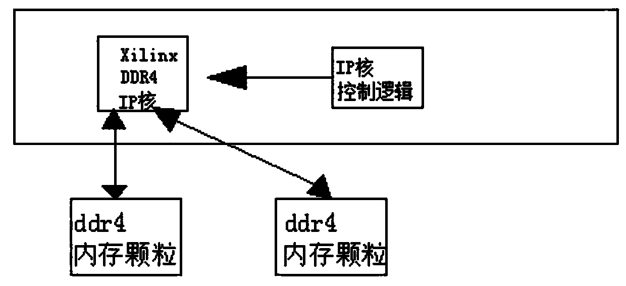
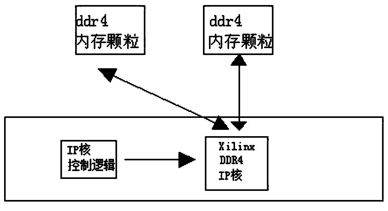
[0031] Such as figure 1 , 2 As shown in , 3, a UFS storage array system based on FPGA control, the system is composed of usb type c interface, several UFS storage chips and FPGA, and the FPGA is equipped with Thunderbolt 3 slave module, Thunderbolt 3master module, MicroBlaze soft core module, address Mapping module, data channel module, write channel ddr controller module and read channel d...


PUM


Abstract

The invention relates to the field of memory design, and particularly provides a UFS storage array system based on FPGA control and a data transmission method. The system is composed of a usb type c interface, a plurality of UFS storage chips and an FPGA. The FPGA is provided with a thunder and lightning 3-slave module, a thunder and lightning 3-master module, a MicroBlaze soft core module, an address mapping module, a data channel module, a write channel ddr controller module and a read channel ddr controller module, and a data transmission method is realized based on the system. Compared with the prior art, in the UFS storage array system based on FPGA control, the full duplex function of the storage array is realized by utilizing the full duplex characteristic of the UFS chip and combining the read-write two-way DDR channel and the thunder and lightning 3 interface in the full duplex working state, so that the storage array adapts to the characteristic of frequent read-write of a modern operation system and has a good popularization value.

Description

technical field [0001] The invention relates to the field of memory design, and specifically provides an FPGA-based UFS storage array system and a data transmission method. Background technique [0002] The Thunderbolt 3 interface is a high-speed interface specification developed by Intel Corporation. The physical interface is compatible with the USB Type C interface, and the maximum bandwidth can reach 40Gbps. More and more computers have this peripheral interface to meet the demand for data interaction speed of future storage devices. Most of the current UFS memory chips are single-chip applications, which basically meet the needs in embedded fields such as mobile phones. However, in some occasions that have high requirements for speed and capacity, it is necessary to use multiple UFS chips to form a storage array. [0003] At present, there is a lack of high-speed storage devices with Thunderbolt 3 interface on the market, and it is impossible to take full advantage of t...

Claims


Application Information

Patent Timeline
Patent Type & Authority Applications(China)
IPC IPC(8): G06F15/78G06F13/12G06F13/16
CPCG06F15/7842G06F13/12G06F13/1668Y02D10/00
Inventor 赵鑫鑫姜凯李朋
Owner SHANDONG INSPUR SCI RES INST CO LTD
Why Eureka
Try Eureka