Regrowth groove-filling GaN-based junction barrier Schottky diode structure and implementation method

A technology of Schottky diode and realization method, applied in the field of microelectronics, can solve the problems of lack of GaN material modification, poor performance of GaN JBS, etc., and achieve the effects of suppressing electric field accumulation effect, improving breakdown electric field, and suppressing reverse leakage

CN111276548AInactive Publication Date: 2020-06-12PEKING UNIV
5 Cites 0 Cited by

Patent Information

Authority / Receiving Office
CN · China
Patent Type
Applications(China)
Current Assignee / Owner
Publication Date
2020-06-12
Estimated Expiration
Not applicable · inactive patent

Smart Images

  • Figure 1
    Figure 1
  • Figure 2
    Figure 2
  • Figure 3
    Figure 3
Patent Text Reader

Abstract

The invention discloses a regrowth groove-filling GaN-based junction barrier Schottky diode structure and a manufacturing method, belongs to the technical field of microelectronics, and relates to manufacturing of power electronic devices. The structure comprises a GaN self-supporting substrate, an n <->-GaN drift region, a P type GaN region, a mask dielectric layer, a groove type structure, a regrown n <->-GaN region, cathode metal and anode metal. The method comprises steps of homoepitaxially extending an n-drift region on the GaN self-supporting substrate, forming a mask dielectric layer and a groove-shaped structure on the structure, re-growing n-GaN to partially or completely fill the groove-shaped structure, and depositing anode and cathode metals. According to the invention, an effective PN junction can be formed on the n-GaN drift region, under reverse bias high voltage, the PN junction can effectively adjust electric field distribution, reduce a metal semiconductor interface electric field, inhibit junction electric leakage and improve the breakdown voltage of the device, and the application range of the GaN-based vertical structure Schottky diode is expanded.
Need to check novelty before this filing date? Find Prior Art

Description

technical field

[0001] The invention belongs to the technical field of microelectronics and relates to the production of power electronic devices Background technique

[0002] In recent years, with the development of material science, GaN substrate materials with high quality and low dislocation density have been gradually commercialized, which facilitates the development of vertical structure devices. GaN substrates obtained by HVPE, sodium fusion and ammonothermal methods Has a very low defect density.

[0003] With the maturity of GaN material growth conditions, homoepitaxial GaN materials on low dislocation density GaN substrates have extremely low defect density, and can strictly control the impurity concentration, thereby growing high-resistance GaN epitaxial materials. The advantages of vertical structure devices in the field of power electronics are prominent. They use high-quality GaN bulk materials for conduction, and are less affected by interface states, which c...

Examples

Embodiment Construction

[0031] In the following, the present invention will be described more fully with reference to the accompanying drawings, in which embodiments and their realization are shown, the described embodiment is only one form of realization in the present invention, that is, the present invention should not be interpreted are limited to the examples set forth herein. Based on the embodiment, the scope of the present invention is fully conveyed to those skilled in the art.

[0032] Hereinafter, exemplary embodiments of the present invention will be described in more detail with reference to the accompanying drawings.

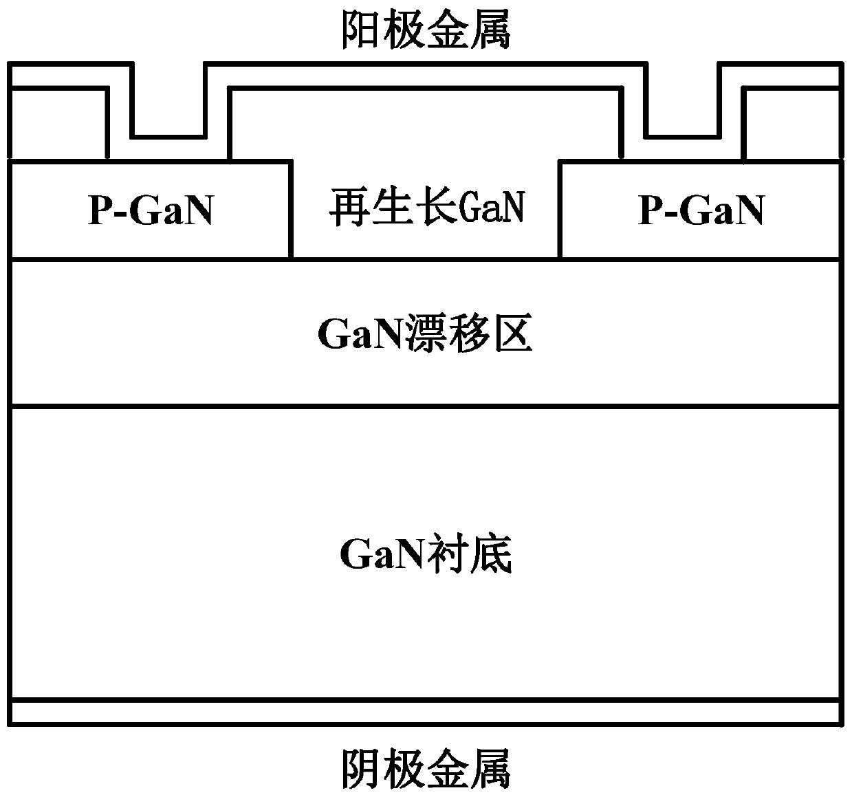
[0033] refer to figure 1 , the device structure from bottom to top includes cathode metal, substrate, n - -GaN drift region, P-type GaN, regrown n - -GaN and anode metal. Its preparation method comprises the following specific steps:

[0034] (1) if Figure 4 As shown, on a GaN free-standing substrate, a layer of n is first grown by MOCVD or MBE - -GaN drift region...