Nor flash erasure interference correction method and Nor flash erasure interference correction device

An N-1, positive integer technology, applied in the field of non-volatile flash memory erasure interference correction, can solve the problems of long time consumption, easy rewriting of physical array data, and high power consumption of the overall erasing operation

Pending Publication Date: 2020-11-27
ZHUHAI CHUANGFEIXIN TECH CO LTD
View PDF6 Cites 1 Cited by
  • Summary
  • Abstract
  • Description
  • Claims
  • Application Information

AI Technical Summary

Problems solved by technology

[0006] In view of this, an embodiment of the present invention provides a Nor flash erasing interference correction method and device to solve the problem of long time consumption of ...

Method used


Image

  • Nor flash erasure interference correction method and Nor flash erasure interference correction device
  • Nor flash erasure interference correction method and Nor flash erasure interference correction device
  • Nor flash erasure interference correction method and Nor flash erasure interference correction device

Examples


Embodiment Construction

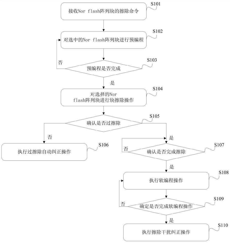
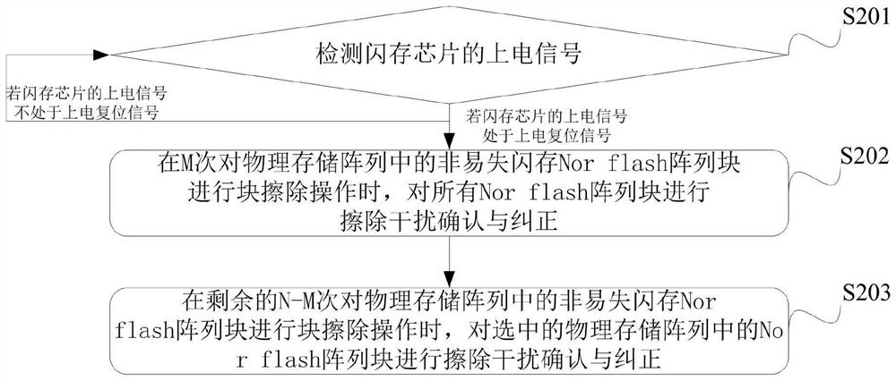
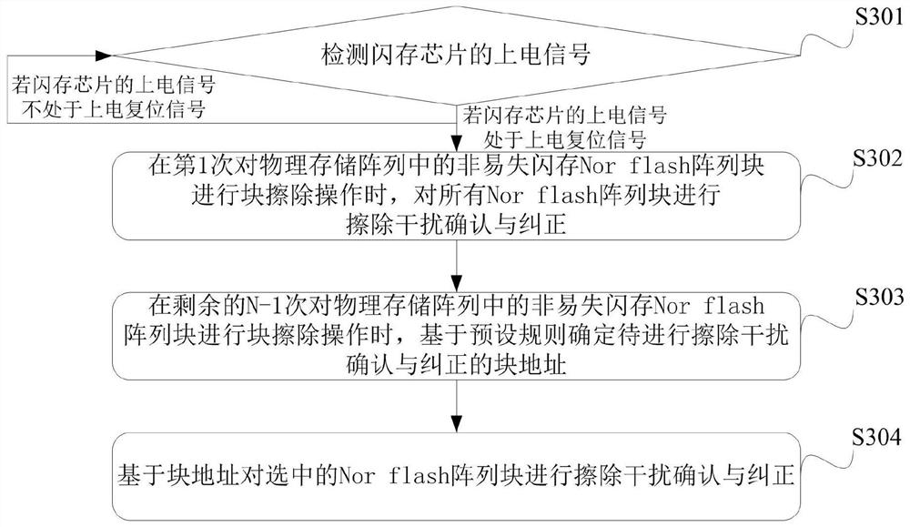
[0053] The following will clearly and completely describe the technical solutions in the embodiments of the present invention with reference to the accompanying drawings in the embodiments of the present invention. Obviously, the described embodiments are only some, not all, embodiments of the present invention. Based on the embodiments of the present invention, all other embodiments obtained by persons of ordinary skill in the art without making creative efforts belong to the protection scope of the present invention.

[0054] In this application, the term "comprises", "comprises" or any other variation thereof is intended to cover a non-exclusive inclusion such that a process, method, article, or apparatus comprising a set of elements includes not only those elements, but also includes none. other elements specifically listed, or also include elements inherent in such a process, method, article, or apparatus. Without further limitations, an element defined by the phrase "com...


PUM


Abstract

The invention provides a Nor flash erasure interference correction method and a Nor flash erasure interference correction device. The method comprises: when a power-on signal of a flash memory chip isin a power-on reset signal, performing erasure interference confirmation and correction on all Nor flash array blocks when the Nor flash array blocks of a nonvolatile flash memory in a physical storage array are subjected to block erasure operation for M times; and performing erasure interference confirmation and correction on the Nor flash array block in the selected physical storage array whenthe Nor flash array block in the physical storage array is subjected to block erasure operation for the remaining N-M times. In the scheme, all Nor flash array blocks are subjected to interference erasing confirmation and correction for at least M times, and in the remaining N-M times, the selected Nor flash array blocks are subjected to interference confirmation and correction each time. Therefore, the time consumption and the power consumption of the whole erasing operation are reduced, and the stored data can be prevented from being rewritten.

Description

technical field [0001] The present invention relates to the technical field of flash memory, in particular to a nonvolatile flash memory (Nor flash) erasure interference correction method and device. Background technique [0002] With the rapid development of portable electronic products, especially after the feature size of the process is less than 65nm, in order to save the chip area, the storage area of ​​the floating gate flash memory chip is generally placed in a physical concentration to form a physical storage matrix. Logically, each The physical storage matrix is ​​divided into multiple Nor flash array blocks based on floating gate technology. Since different Nor flash array blocks are located on the same P-type substrate (PWELL), when erasing a Nor flash array block in the same physical storage array, because the Nor flash array block and the surrounding Nor flash The drain region, the source region and the P well of the array block are connected, and the remaining...

Claims


Application Information

Patent Timeline
IPC IPC(8): G06F3/06G06F12/02G06F11/10
CPCG06F3/062G06F3/0625G06F3/0652G06F3/064G06F3/0679G06F12/0246G06F11/1004Y02D10/00
Inventor 王志刚李弦叶谦王少龙张文豪
Owner ZHUHAI CHUANGFEIXIN TECH CO LTD
Why Eureka
Try Eureka