Display assembly and display device

A technology for display components and display devices, which is applied to identification devices, electrical components, electrical solid devices, etc., can solve problems such as occupying external space, achieve narrow frame design, reduce processing procedures and costs, and save processing procedures.

Pending Publication Date: 2021-12-03
HKC CORP LTD
View PDF0 Cites 2 Cited by
  • Summary
  • Abstract
  • Description
  • Claims
  • Application Information

AI Technical Summary

Problems solved by technology

Because the base substrate and the film need to reserve space for accommodating and connecting the flexible cable FPC, and part of the flexible cable FPC on the side of the substrate substrate will occupy a part of the external space, resulting in displays using Mini-LED chips as light sources Has a wider nondisplay border

Method used


Image

  • Display assembly and display device
  • Display assembly and display device
  • Display assembly and display device

Examples


no. 1 example

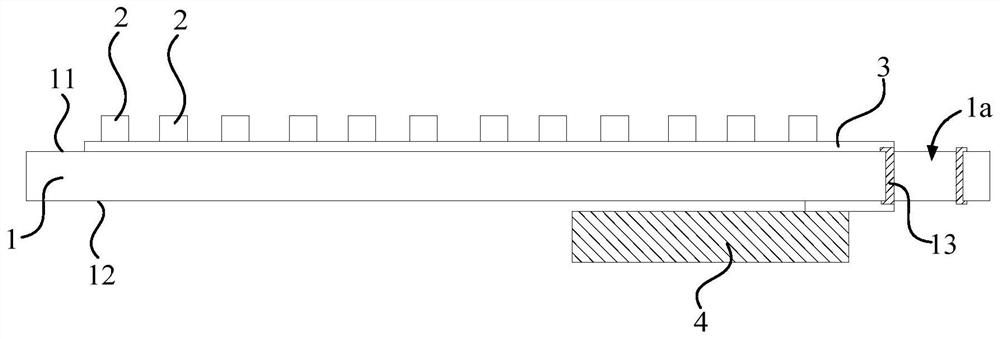
[0060] Such as Figures 1 to 3 As shown, each channel 1a provided on the glass substrate 1 is a through-hole structure, and a plurality of through-hole structures are disposed adjacent to the outer wall of the glass substrate 1 .

[0061] In this embodiment, each channel 1a is designed as a through-hole structure, and the through-hole structure may be a circular hole or an oval hole, so as to facilitate the processing of the through-hole structure. The glass substrate 1 can be a square structure, and the glass substrate 1 has four outer sidewalls arranged in pairs. A plurality of through hole structures can be arranged adjacent to the same outer sidewall of the glass substrate 1, or can be arranged adjacent to different outer sidewalls respectively. By arranging a plurality of through-hole structures adjacent to the outer wall of the glass substrate 1, each through-hole structure will be located at the edge of the glass substrate 1, so that on the basis of realizing the arrang...

no. 2 example

[0063] combine figure 2 , Figure 5 as well as Figure 7 As shown, each channel 1 a provided on the glass substrate 1 is a notch structure, and each notch structure is provided on the outer wall of the glass substrate 1 .

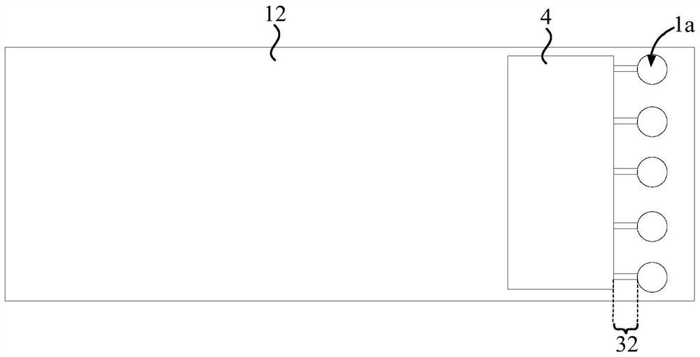
[0064] In this embodiment, each notch structure is opened on the outer sidewall of the glass substrate 1 , and each notch structure is disposed through the first loading surface 11 , the second loading surface 12 and the outer sidewall of the glass substrate 1 . The conductive layer 13 is provided on the inner sidewall of the notch structure, and is used to realize the electrical connection between the driving circuit 3 and the driving module 4 . By designing the channel 1a as a notch structure and setting each notch structure on the outer wall of the glass substrate 1, on the basis of realizing the arrangement of a plurality of light-emitting elements 2 and driving lines 3, the number of holes in each through hole of the glass substrate 1 can be reduced...

no. 3 example

[0070] Such as Figure 8 As shown, the glass substrate 1 is a square structure, the glass substrate 1 has two first sides 14 and two second sides 15, and the first sides 14 and the second sides 15 are alternately connected; the channel 1a includes a plurality of The first channel 1a1 and the plurality of second channels 1a2, the inner wall of each first channel 1a1 and the inner wall of each second channel 1a2 are provided with a conductive layer 13, and each conductive layer 13 is electrically connected to the drive module 4; A channel 1a1 is adjacent to a first side 14 and arranged at intervals along the extending direction of the first side 14; a plurality of second channels 1a2 is adjacent to a second side 15 and arranged at intervals along the extending direction of the second side 15 The driving circuit 3 includes a plurality of scanning lines 34 and a plurality of data lines 35 arranged on the first carrier surface 11, and each data line 35 is connected to a plurality o...


PUM

PropertyMeasurementUnit
widthaaaaaaaaaa

Abstract

The invention discloses a display assembly and a display device. The display assembly comprises a glass substrate, a plurality of light-emitting elements, a driving circuit and a driving module, the glass substrate is provided with a first carrying surface, and the side, opposite to the first carrying surface, of the glass substrate is provided with a second carrying surface; the glass substrate is provided with a channel penetrating through the first carrying surface and the second carrying surface, and the inner wall of the channel is provided with a conductive layer; the plurality of light-emitting elements are arranged on the first carrying surface; the driving circuit is at least partially arranged on the first carrying surface and is connected with the conductive layer and the plurality of light-emitting elements; and the driving module is arranged on the second carrying surface and is electrically connected with the conductive layer. The display assembly provided by the invention can realize a narrow frame design.

Description

technical field [0001] The present invention relates to the field of display technology, in particular to a display component and a display device. Background technique [0002] Mini-LED (Micro Light Emitting Diode) chip is an LED chip with a width of about 100 μm. Mini-LED chips are used in the display field because of their advantages such as high brightness, high color saturation, and local dimming. [0003] In related technologies, the Mini-LED chip is used as a light source on a thin film integrated with a driving circuit, and is connected to the driving circuit. ) from the outside of the edge of the substrate to the back of the substrate to connect the drive module, and the drive module transmits control signals to the drive circuit on the film through the flexible cable FPC to control the corresponding Mini-LED chip on and off. Because the base substrate and the film need to reserve space for accommodating and connecting the flexible cable FPC, and part of the flexib...

Claims


Application Information

Patent Timeline
Patent Type & Authority Applications(China)
IPC IPC(8): H01L25/16G09F9/33
CPCH01L25/167G09F9/33
Inventor 何海龙康报虹
Owner HKC CORP LTD
Why Eureka
Try Eureka