Display apparatus

A display device and grid line technology, applied in static indicators, nonlinear optics, instruments, etc., can solve problems such as the limitation of occupied area, and achieve the effect of reducing the number of logic elements, reducing the area, and narrowing the frame

Inactive Publication Date: 2006-09-06
SONY CORP
View PDF0 Cites 7 Cited by
  • Summary
  • Abstract
  • Description
  • Claims
  • Application Information

AI Technical Summary

Problems solved by technology

Therefore, the occupied area of ​​the pixel array constituting the display screen is partially limited due to the disadvantage of an increase in the required surface area of ​​the LCD panel, thus creating another problem to be solved

Method used


Image

  • Display apparatus
  • Display apparatus
  • Display apparatus

Examples


Embodiment Construction

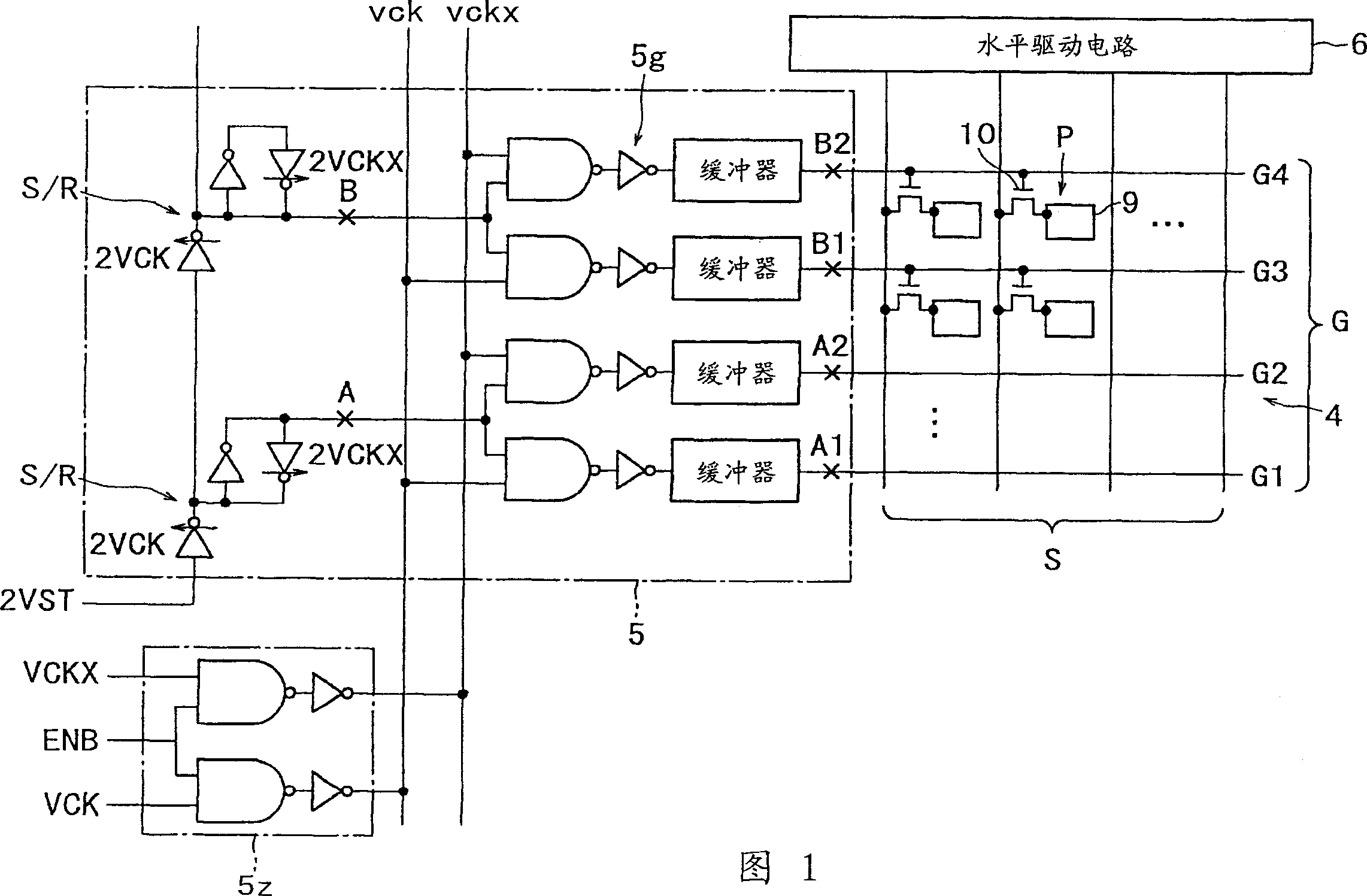
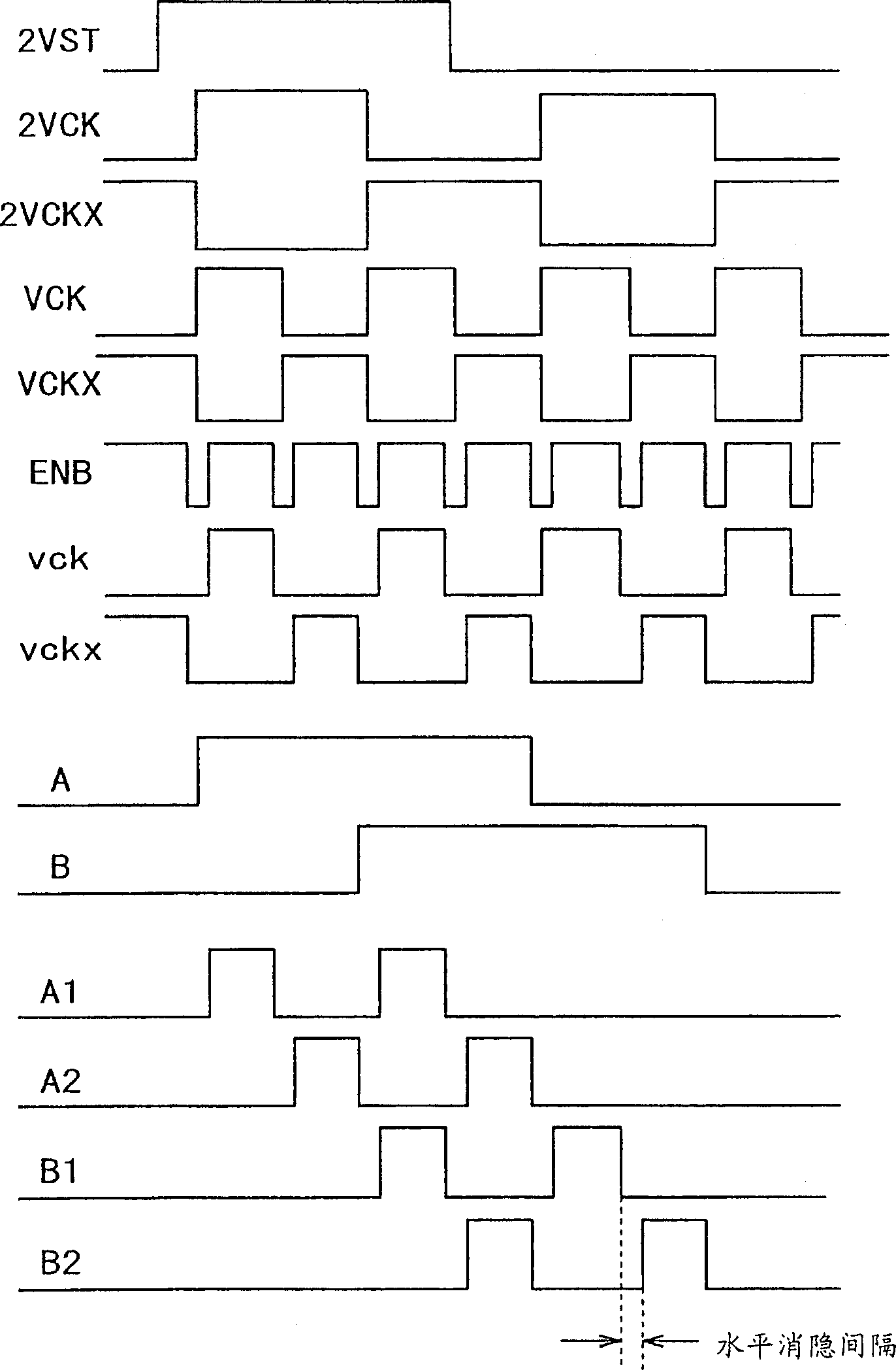
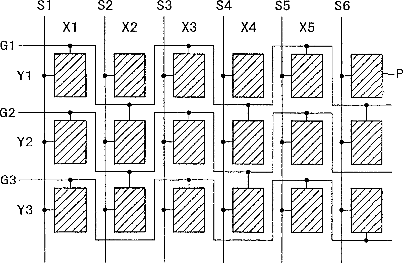
[0015] Embodiments of the present invention will be described below with reference to the accompanying drawings. FIG. 1 is a circuit diagram showing a specific structure of a display device of the present invention. As shown in the figure, the display device basically includes a pixel array 4, a vertical driving circuit 5 and a horizontal driving circuit 6, which are formed in an integrated manner by thin film transistors and the like on one substrate. The pixel array 4 includes a plurality of gate lines G, a plurality of signal lines S, and pixels P arranged at intersections of the gate lines G and the signal lines S to form a matrix. In this example, each pixel P is composed of a pixel electrode 9 and a thin film transistor 10 . Although not shown, an opposite electrode is formed at a position opposite to the pixel electrode 9 with, for example, a liquid crystal as an electro-optical substance interposed between these two electrodes. The gate of the thin film transistor 10...


PUM


Abstract

A display device so improved as to reduce the size of a peripheral driving circuit incorporated therein. The display device comprises, on one substrate, a pixel array (4), a vertical driving circuit (5) for sequentially selecting pixels (P) via gate lines (G), and a horizontal driving circuit (6) for writing image signals in the selected pixels (P) via signal lines (S). The vertical driving circuit (5) has shift registers (S / R) so disposed that one stage thereof corresponds to at least two gate lines (G), and outputting shift pulses sequentially from the respective stages thereof; gate circuits (5g) for generating drive pulses by extracting, in response to the shift pulses, the clock pulses supplied thereto externally, and outputting the drive pulses to the gate lines (G) to thereby execute sequential selection of the the pixels (P); and a shaping means (5z) for shaping the clock pulses previously in accordance with a horizontal blanking pulse supplied externally in synchronism with a horizontal blanking interval, and supplying the shaped clock pulses to the gate circuits (5g).

Description

technical field [0001] The present invention relates to an active matrix type display device represented by LCD, in particular to a structure of a vertical driving circuit for driving a pixel matrix array. Background technique [0002] Figure 8 is a perspective view showing a general structure of an active matrix type display device. As shown in the figure, a conventional display device has a panel configuration consisting of a pair of substrates 1, 2 and a liquid crystal 3 sandwiched therebetween. The pixel array 4 and the driving circuit are formed on the lower substrate 1 in an integrated manner. The driving circuit is divided into a vertical driving circuit 5 and a horizontal driving circuit 6 . Also, terminals 7 for external connection are formed on the peripheral upper end of the substrate. Each terminal 7 is connected to the vertical drive circuit 5 and the horizontal drive circuit 6 through wiring 8 . Gate lines G and signal lines S are formed in the pixel array...

Claims


Application Information

Patent Timeline
Patent Type & Authority Patents(China)
IPC IPC(8): G09G3/36G09G3/20G02F1/133G02F1/1345
CPCG09G3/3677G09G3/3614G09G2310/0281G02F1/133
Inventor 山下淳一内野胜秀
Owner SONY CORP
Why Eureka
Try Eureka