Organic electroluminescent display device and its manufacture and electronic apparatus

An electroluminescence display and display device technology, applied in the direction of electroluminescence light source, electric light source, lighting device, etc., can solve the problems of long time, organic EL element damage, display panel sealing damage, etc., to reduce air intrusion the danger, the effect of reducing the path

Inactive Publication Date: 2005-05-11
SEIKO EPSON CORP
View PDF1 Cites 4 Cited by
  • Summary
  • Abstract
  • Description
  • Claims
  • Application Information

AI Technical Summary

Problems solved by technology

In the aforementioned Patent Document 1, although a polyimide substrate is used as one of the substrates, the polyimide substrate has a problem of insufficient gas barrier, and there is a risk of damage to the organic EL element.
[0008] In addition, if a glass substrate or other substrate having a thermal expansion coefficient different from that of the polyimide substrate is used as the other substrate, the sealability of the display panel may be damaged due to the difference in thermal expansion coefficient of each substrate, and the organic EL element may be damaged.
[0009] In addition, even if a glass substrate with barrier properties is used as one of the above-mentioned substrates, it is difficult to form a large number of through holes on the glass substrate in the prior art, and there is a problem that it takes a long time to form them.

Method used


Image

  • Organic electroluminescent display device and its manufacture and electronic apparatus
  • Organic electroluminescent display device and its manufacture and electronic apparatus
  • Organic electroluminescent display device and its manufacture and electronic apparatus

Examples


Embodiment Construction

[0041] Below, refer to Figure 1 to Figure 6 , the organic electroluminescent display device (hereinafter, referred to as organic EL display device), large-scale organic EL display device and method for manufacturing the organic EL display device of the present invention will be described.

[0042] In addition, in each drawing used for the following description, the scale of each member is changed suitably so that each part may become a recognizable size.

[0043] (Organic EL device)

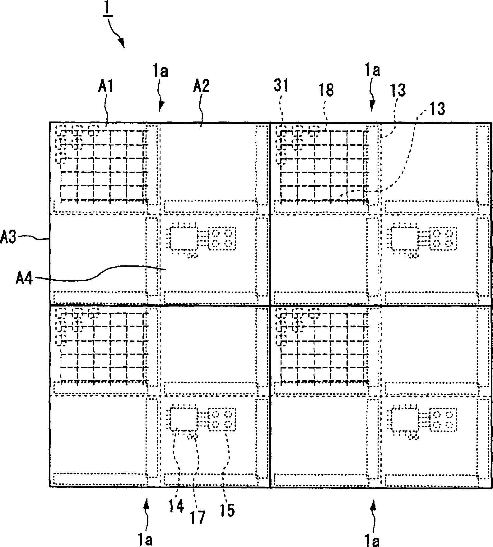
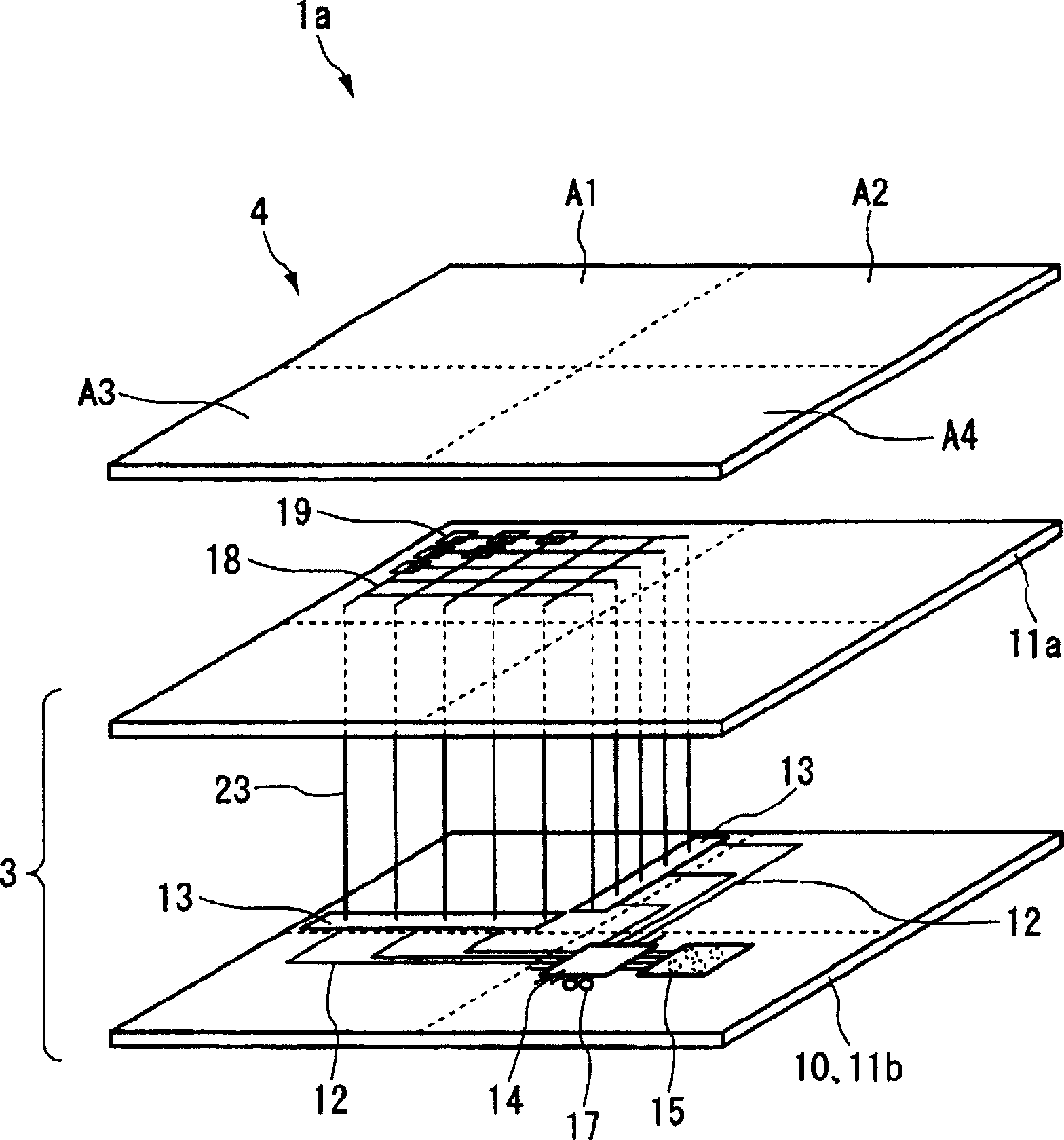
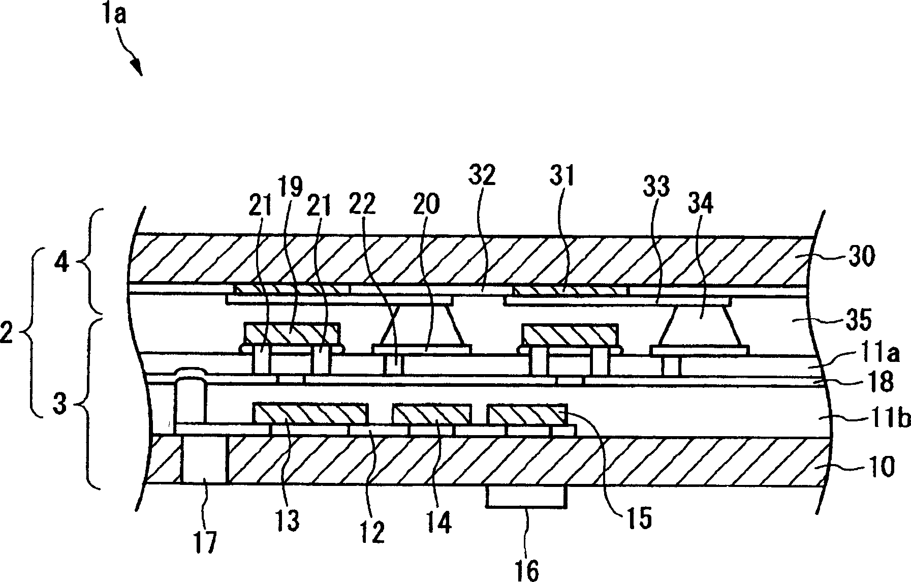
[0044] figure 1 It is a plan view showing the overall structure of the organic EL display device of the present invention. figure 2 It is an exploded perspective view of the organic EL display device of the present invention. image 3 It is a sectional view of main parts of the organic EL display device of the present invention. figure 1 and figure 2 Parts with repeating structures in , represent part of it and omit other parts.

[0045] Such as figure 1 As shown, the organic EL display...


PUM


Abstract

The present invention provides an organic EL display device, a method for manufacturing the organic EL display device, and a large-scale organic electroluminescent display device that can prevent damage to EL elements and can be easily tiled so that the seam between the organic EL display devices is not conspicuous. devices and electronic equipment. Organic electroluminescent display device (1a): having an electroluminescent substrate (4) including an electroluminescent element (31) emitting light, including a thin film transistor (19) for controlling the current supplied to the electroluminescent element (31) The thin-film transistor substrate (3), the electroluminescent substrate (4) and the thin-film transistor substrate (3) are arranged oppositely, it is characterized in that, between the electroluminescent substrate (4) and the thin-film transistor substrate (3) is arranged A first control mechanism (13) for controlling the thin film transistor (19).

Description

technical field [0001] The invention relates to an organic electroluminescent display device, a method for manufacturing the organic electroluminescent display device, a large-scale organic electroluminescent display device and electronic equipment. Background technique [0002] In recent years, display panels using organic electroluminescent elements (hereinafter, referred to as organic EL elements) can realize high-quality display by driving the organic EL elements with thin film transistors (hereinafter, referred to as TFTs). In particular, a display panel using an organic EL element, since the organic EL element is a solid element, is easier to seal the end face of the display panel than a display panel using a liquid crystal, and is suitable for arranging a plurality of display panels in parallel for large-scale Tiling (tiling) technology. [0003] When performing the above-mentioned tiling of the display panel, it is difficult to secure a position for mounting a drive...

Claims


Application Information

Patent Timeline
Patent Type & Authority Applications(China)
IPC IPC(8): H01L51/50H01L27/32H05B33/04H05B33/10H05B33/12H05B33/14H05B44/00
CPCH10K59/127H10K59/13H10K59/18H05B33/04H05B33/10
Inventor 小枝周史
Owner SEIKO EPSON CORP
Why Eureka
Try Eureka