Display panel, method of manufacturing display panel, and display device

a display panel and display technology, applied in the field of display panel technology, to achieve the effect of intelligent adjustment of display contras

Active Publication Date: 2019-05-28
HKC CORP LTD +1
View PDF4 Cites 0 Cited by
  • Summary
  • Abstract
  • Description
  • Claims
  • Application Information

AI Technical Summary

Benefits of technology

[0008]In view of the above-mentioned drawbacks of the prior art, the technical problem to be solved in the application is to provide a display panel, a method of manufacturing a display panel, and a display device. The display panel is able to intelligently adjust the display contrast according to the brightness of the external environment.
[0016]In the application, a color photoresist is coated on a finished array substrate (ARRAY) to form a color filter layer. As a result, it is possible to solve the problem that the aperture ratio of the conventional color filter is low. At the same time, a photo-sensor is disposed corresponding to the display region of the array substrate, so that the brightness of the external environment of the display region can be perceived through the photo-sensor. In particular, changes in the strength of external light can be perceived. As a result, when the light is strong, the display device can automatically adjust to improve the brightness and enhance the contrast so as to avoid the image from being too dark and not clear. When the light is weak, the display device can correspondingly lower the brightness and reduce the contrast so as to avoid the image from being too bright and dazzling, which would damage eyes. Accordingly, the display device is capable of better and more intelligent adjustment in the display contrast and the display performance.

Problems solved by technology

In view of the above-mentioned drawbacks of the prior art, the technical problem to be solved in the application is to provide a display panel, a method of manufacturing a display panel, and a display device.

Method used


Image

  • Display panel, method of manufacturing display panel, and display device
  • Display panel, method of manufacturing display panel, and display device

Examples


Embodiment Construction

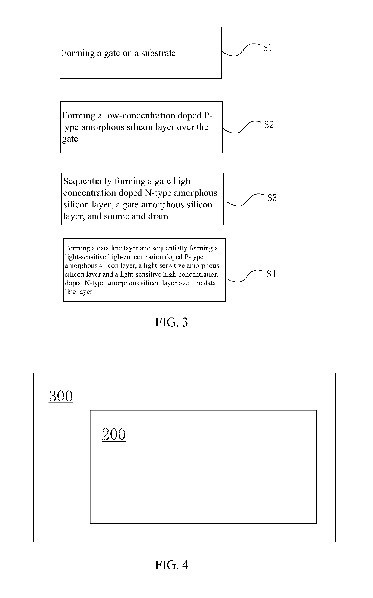
[0025]In order to make those skilled in the art better understand the technical solution of the application, the technical solution in the embodiments of the application will be clearly and completely described in connection with the drawings in the embodiments of the application. It is apparent that the described embodiments are merely parts of the embodiments of the application, rather than all embodiments. Based on the embodiments of the application, all other embodiments obtained by those skilled in the art without inventive efforts are within the scope of the application.

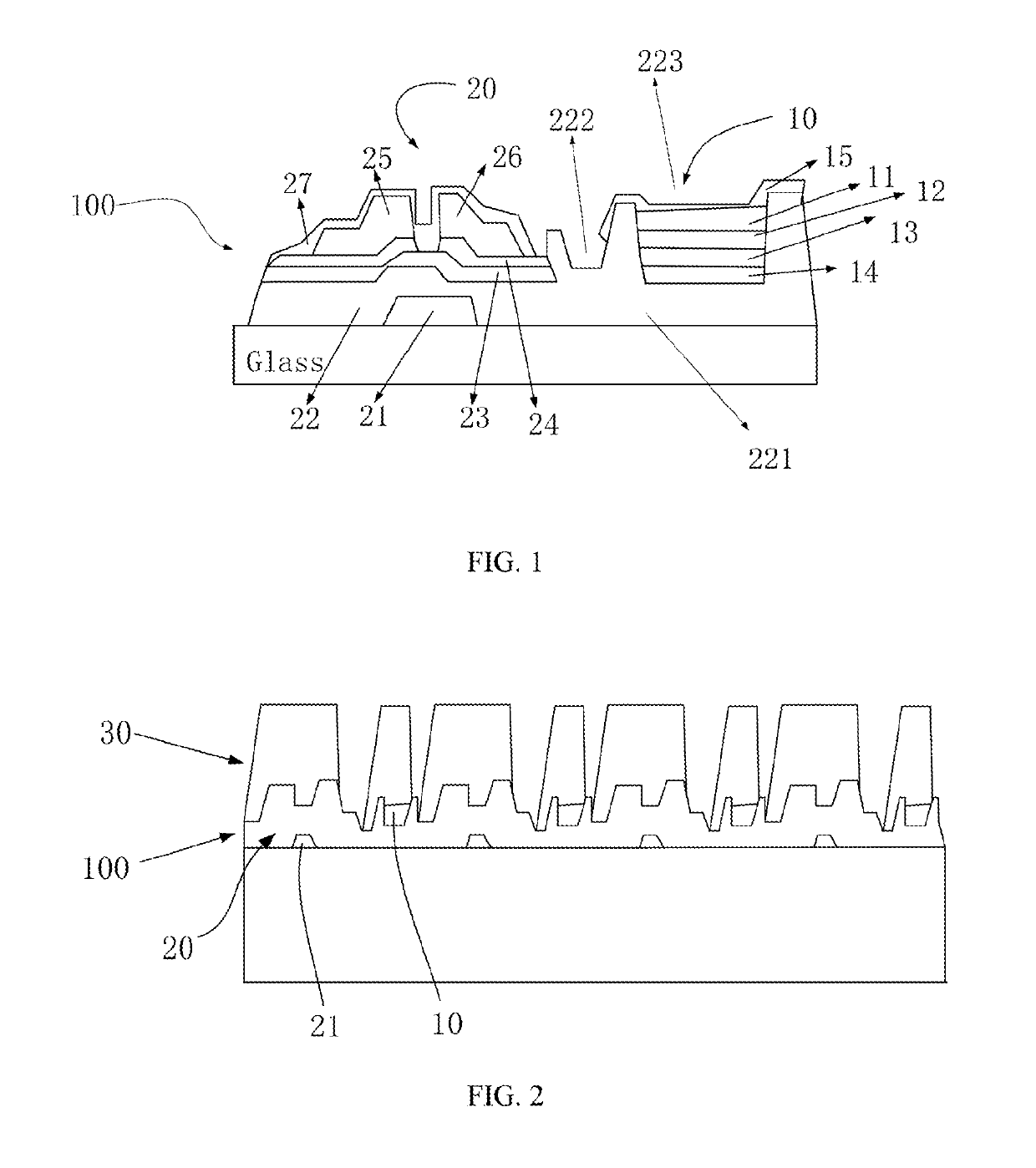
[0026]FIG. 1 is a schematic view showing an array substrate of a display panel of the application. FIG. 2 is an overall schematic view showing a display panel of the application. Referring to FIGS. 1 and 2, the application discloses a display panel comprising an array substrate 100 and a color filter layer 30 on the array substrate 100. The array substrate 100 comprises a display region and a non-display region...


PUM

PropertyMeasurementUnit
concentrationaaaaaaaaaa
conductiveaaaaaaaaaa
transparentaaaaaaaaaa

Abstract

A display panel, a method of manufacturing a display panel, and a display device are provided. The display panel includes an array substrate and a color filter layer on the array substrate. The array substrate includes a display region and a non-display region. The display region includes a photo-sensor.

Description

BACKGROUND OF THE INVENTION[0001]Field of the Invention[0002]The invention relates to a display panel technology, and in particular to a display panel, a method of manufacturing a display panel, and a display device.[0003]Description of the Related Art[0004]With the development and progress of technology, liquid crystal display has advantages including a thin body, low power consumption, and low radiation. Accordingly, the liquid crystal display becomes the mainstream display products and has been widely used. Most of the liquid crystal displays on the market are backlit liquid crystal display, comprising a liquid crystal panel and a backlight module. The liquid crystal panel works by placing liquid crystal molecules between two parallel glass substrates and applying a driving voltage to the two glass substrates to control the direction of rotation of the liquid crystal molecules. As a result, the light from the backlight module is reflected to generate images.[0005]Thin Film Transi...

Claims


Application Information

Patent Timeline
Patent Type & Authority Patents(United States)
IPC IPC(8): H01L27/00G02F1/1368H01L29/786H01L27/12H01L31/105G02F1/133H01L29/00G02F1/1362
CPCG02F1/13318G02F1/1368H01L27/124H01L27/127H01L27/1222H01L27/1255H01L29/78666H01L31/1055H01L27/1248G02F2202/103G02F2001/13312G02F2001/136222H01L31/153G02F2201/58G02F1/13312G02F1/136222G02F1/136295
Inventor CHO, EN-TSUNGTIAN, YIQUN
Owner HKC CORP LTD
Why Eureka
Try Eureka