

Semiconductor device with wire bond inductor and method
- Summary
- Abstract
- Description
- Claims
- Application Information
AI Technical Summary
Problems solved by technology
Method used
Image

Examples
Example
DETAILED DESCRIPTION OF THE DRAWINGS
[0016] In the figures, elements having the same reference number have similar functionality.
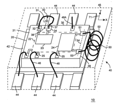
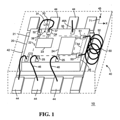
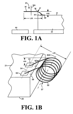
[0017]FIG. 1 is an isometric view of a semiconductor device configured as an integrated circuit (IC) 10 that includes a semiconductor die 20 and wire bond inductors 30 and 50 all housed in a semiconductor package 40. In one embodiment, integrated circuit 10 functions as a high frequency oscillator for use in a dual-band wireless communications device (not shown). Accordingly, integrated circuit 10 generates a high frequency signal operating at either about eight hundred megahertz or about 2.4 gigahertz.
[0018] Semiconductor package 40 includes a die attach flag 42 for mounting semiconductor die 20. A plurality of leads 44 provide electrical connections to external circuitry (not shown). A plurality of wire bonds 46 and a wire bond 46A are attached between leads 44 and a plurality of bonding pads 25 to route signals between the external circuitry and semic...
PUM
 Abstract
Description
Claims
Application Information