Organic light emitting display device

a light-emitting display and organic technology, applied in the direction of static indicating devices, discharge tubes luminescnet screens, instruments, etc., can solve the problem of finely patterning each sub-pixel according to the deposition process using a fine metal mask, and achieve the effect of increasing the aperture ratio and increasing the lifespan

Active Publication Date: 2013-01-03
SAMSUNG DISPLAY CO LTD
View PDF15 Cites 42 Cited by
  • Summary
  • Abstract
  • Description
  • Claims
  • Application Information

AI Technical Summary

Benefits of technology

[0008]Embodiments of the present invention provide an organic light emittin

Problems solved by technology

However, there is a limitation in finely patterning each of the sub

Method used


Image

  • Organic light emitting display device
  • Organic light emitting display device
  • Organic light emitting display device

Examples


Embodiment Construction

[0038]Hereinafter, embodiments of an organic light emitting display device according to the present invention will be described with reference to accompanying drawings.

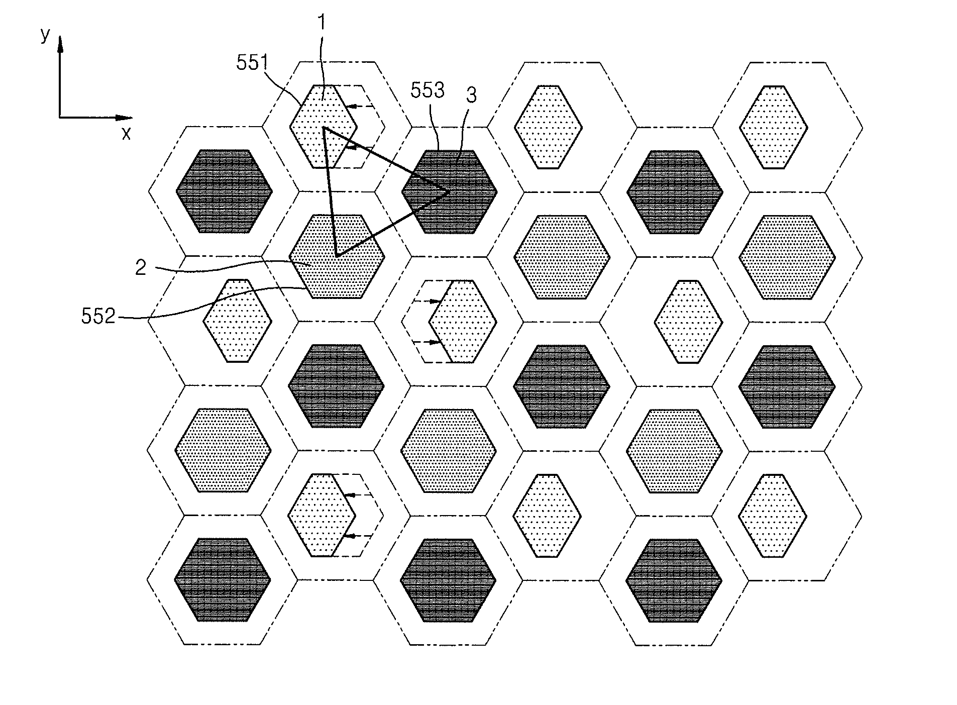
[0039]FIG. 1 is a plan view of sub-pixels in an organic light emitting display device according to an embodiment of the present invention.

[0040]Referring to FIG. 1, the organic light emitting display device according to the present embodiment includes sub-pixels, with each of the sub-pixels being substantially hexagon-shaped (e.g., six sided) and arranged in a substantially hexagonal structure.

[0041]Each of the sub-pixels includes a pixel circuit including an organic light emitting device and a thin film transistor.

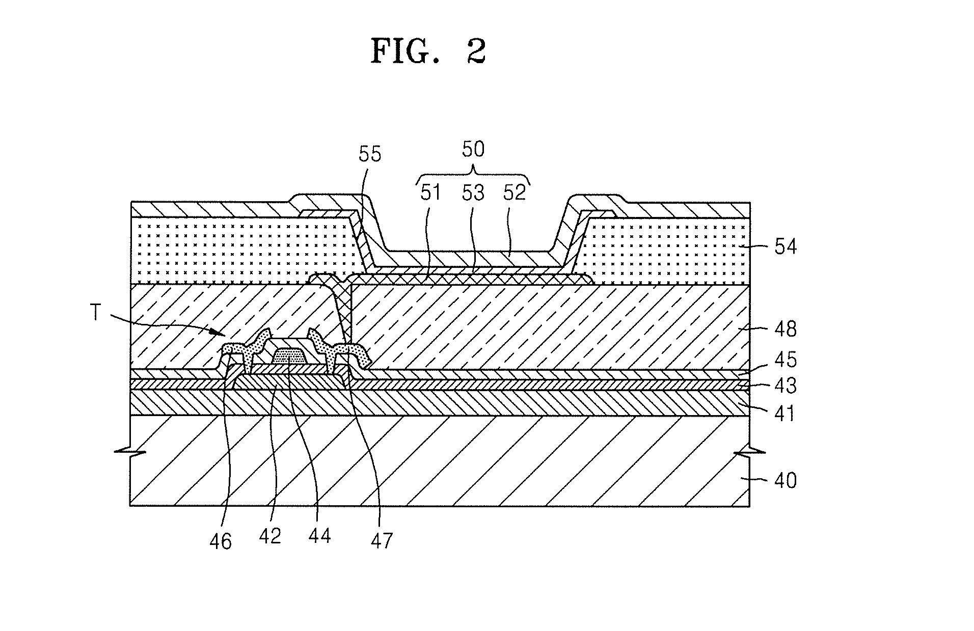
[0042]FIG. 2 is a cross-sectional view of one of the sub-pixels of the embodiment shown in FIG. 1.

[0043]As shown in FIG. 2, a thin film transistor T is formed on a substrate 40, and an organic light emitting device 50 that is electrically coupled to the thin film transistor T is located on the substrate 40....


PUM


Abstract

An organic light emitting display device includes a plurality of sub-pixels arranged in a substantially hexagonally-shaped structure, each of the sub-pixels including a corresponding one of a plurality of organic light emitting devices, wherein the plurality of sub-pixels includes a plurality of first sub-pixels for emitting light of a first color, a plurality of second sub-pixels for emitting light of a second color, and a plurality of third sub-pixels for emitting light of a third color, and wherein centers of adjacent ones of the first, second, and third sub-pixels form a triangle having one of three sides that is shorter than the other two of the sides.

Description

CROSS-REFERENCE TO RELATED PATENT APPLICATION[0001]This application claims priority to and the benefit of Korean Patent Application No. 10-2011-0065141, filed on Jun. 30, 2011, in the Korean Intellectual Property Office, the disclosure of which is incorporated herein in its entirety by reference.BACKGROUND[0002]1. Field[0003]Embodiments of the present invention relate to an organic light emitting display device.[0004]2. Description of Related Art[0005]Organic light emitting display devices are self-emissive displays that emit light by electrically exciting organic compounds, and are being considered as next generation display devices that may address problems of liquid crystal display devices, as organic light emitting display devices may operate with low voltage, may have a thin profile, and have wide viewing angles and fast response speeds. Therefore, demands for organic light emitting display devices with high resolution are increasing.[0006]A light emission layer in each of sub-...

Claims


Application Information

Patent Timeline
IPC IPC(8): H01J1/63
CPCH01L27/3216H05B33/02H01L27/3218G09G2300/0452G09G3/3208H10K59/352H10K59/353H10K50/805H10K2102/3026
Inventor KO, JUNG-WOO
Owner SAMSUNG DISPLAY CO LTD
Why Eureka
Try Eureka