Liquid crystal display

a liquid crystal display and display technology, applied in non-linear optics, instruments, optics, etc., can solve the problems of reducing driving efficiency, reducing entire luminance, and difficulty in accurately expressing grays in low gray regions, so as to prevent deterioration of luminance, accurate expression of grays, and preventing variation of pixel voltage

Active Publication Date: 2016-12-01
SAMSUNG DISPLAY CO LTD
View PDF2 Cites 1 Cited by
  • Summary
  • Abstract
  • Description
  • Claims
  • Application Information

AI Technical Summary

Benefits of technology

[0018]According to the embodiment, it is possible to accurately express a gray in a low gray region while making lateral visibility close to front visibility, to prevent deterioration of luminance compared to an applied driving voltage, to prevent variation of a pixel voltage by two signal wires for inputting signals having different polarities, and to prevent a brightness difference between adjacent pixels by preventing a difference between aperture ratios of the adjacent pixels.

Problems solved by technology

In a case where one pixel is divided into two subpixels and a voltage of any one subpixel thereof is lowered, as a result, voltages of the two subpixels are different from each other, luminance of the lateral side is increased compared with the front in a low gray, and thus it is difficult to accurately express a gray in a low gray region, and the entire luminance is lowered as compared with the applied pixel voltage, and as a result, there is a problem in that driving efficiency is lowered.
Further, when a difference between aperture ratios of adjacent pixels occurs, a brightness difference between the adjacent pixels may occur.

Method used


Image

  • Liquid crystal display
  • Liquid crystal display
  • Liquid crystal display

Examples


Embodiment Construction

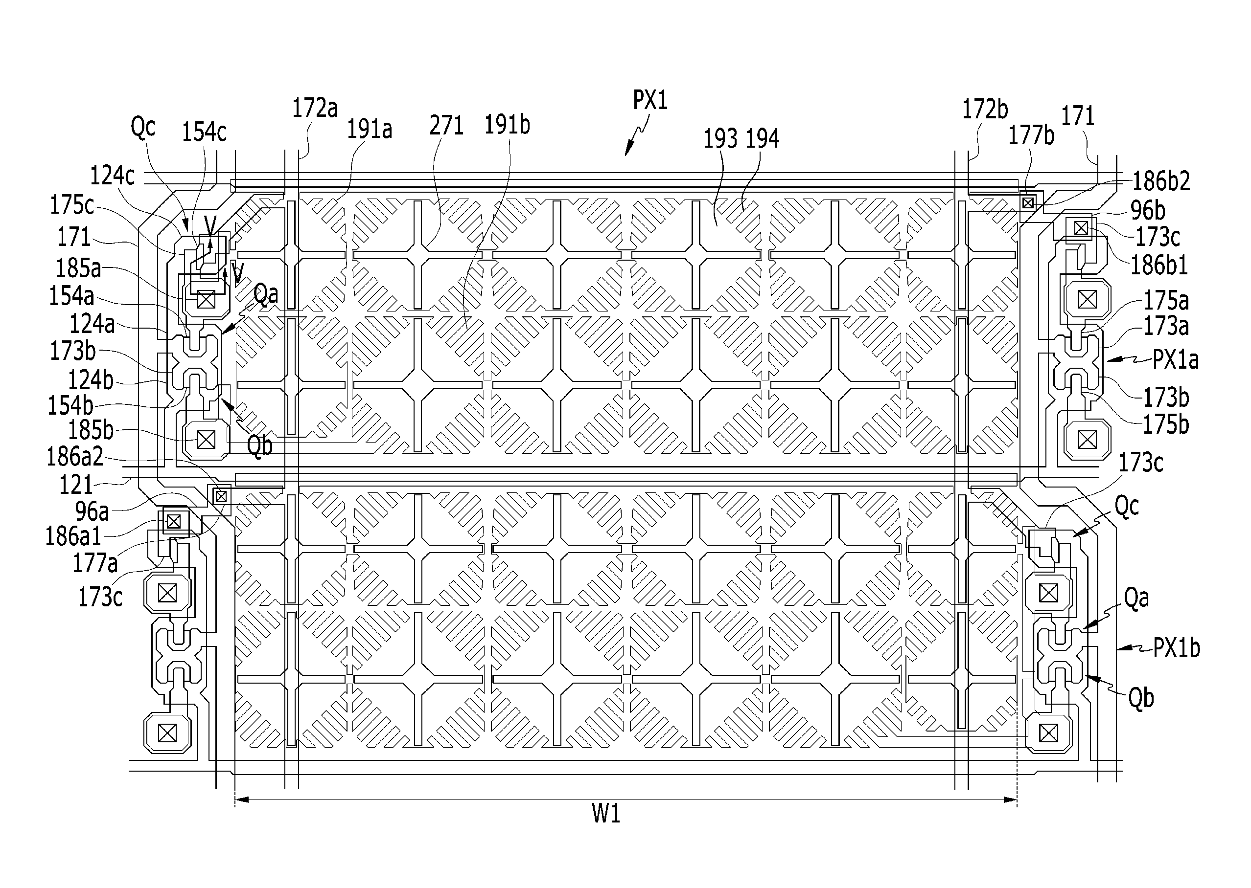
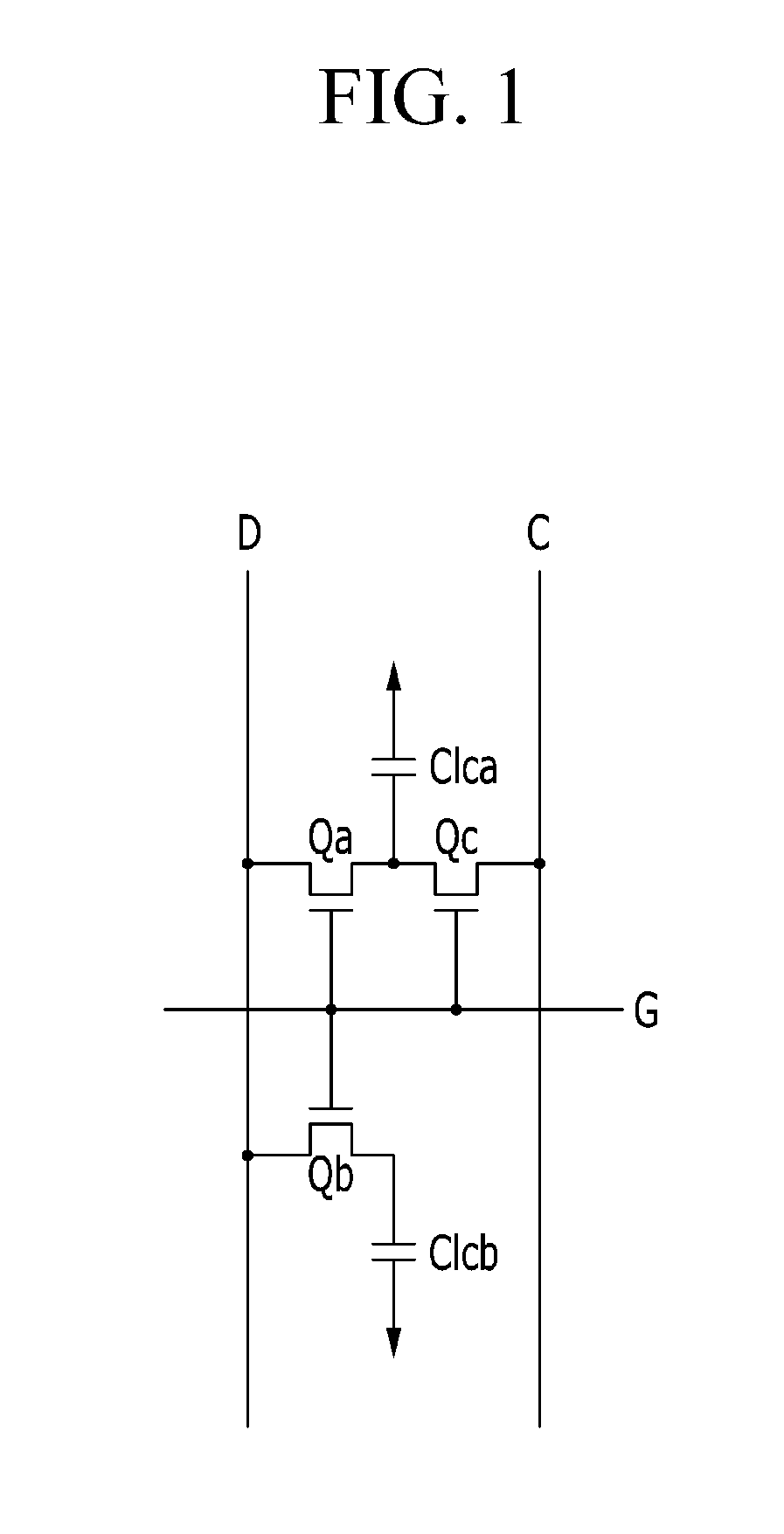
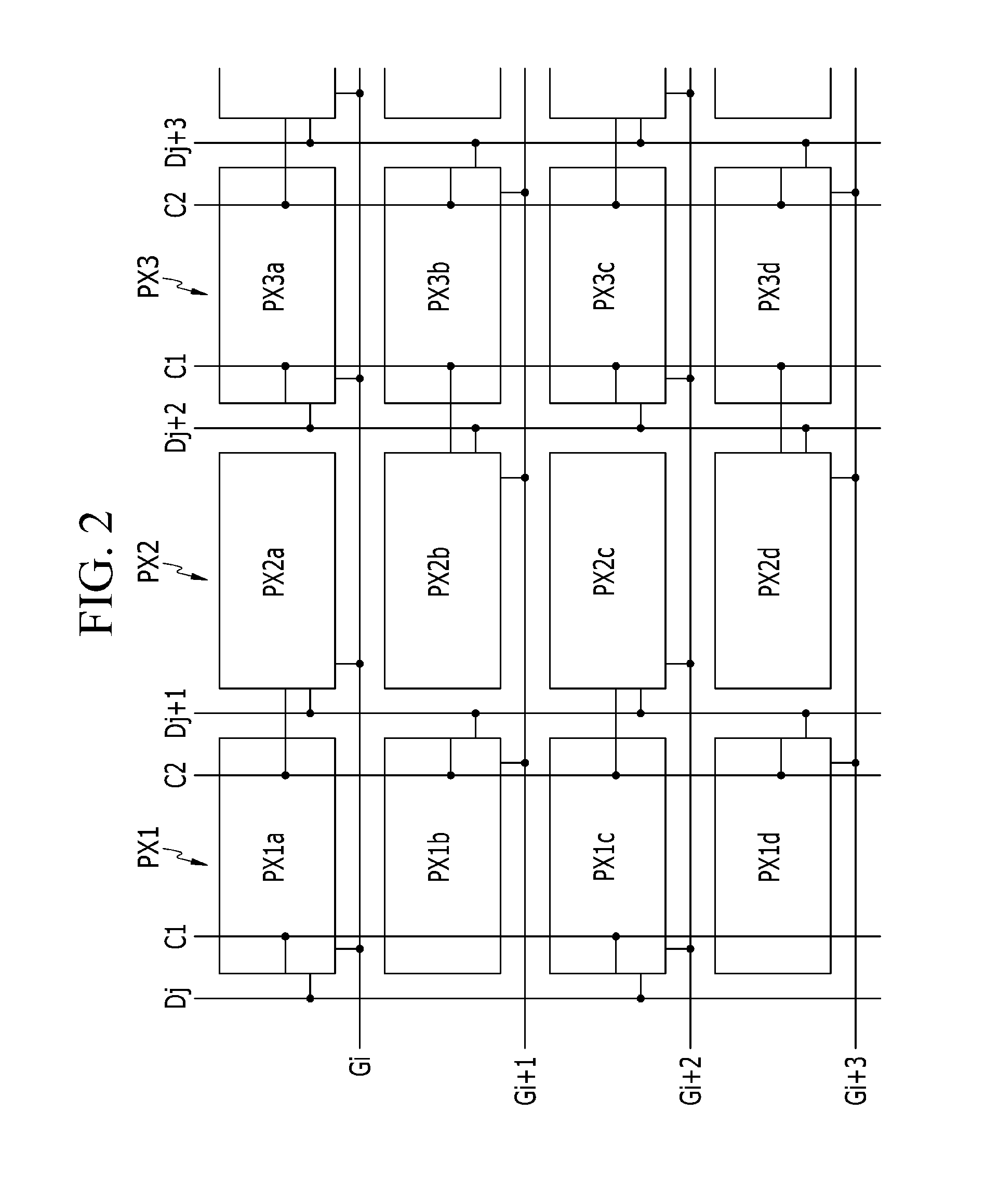
[0027]The invention will be described more fully hereinafter with reference to the accompanying drawings, in which exemplary embodiments of the invention are shown. As those skilled in the art would realize, the described embodiments may be modified in various different ways, all without departing from the spirit or scope of the invention.

[0028]In the drawings, the thickness of layers, films, panels, regions, etc., are exaggerated for clarity. Like reference numerals designate like elements throughout the specification. It will be understood that when an element such as a layer, film, region, or substrate is referred to as being “on” another element, it can be directly on the other element or intervening elements may also be present. In contrast, when an element is referred to as being “directly on” another element, there are no intervening elements present.

[0029]It will be understood that, although the terms “first,”“second,”“third” etc. may be used herein to describe various eleme...


PUM

PropertyMeasurementUnit
polaritiesaaaaaaaaaa
areaaaaaaaaaaa
widthaaaaaaaaaa

Abstract

A liquid crystal display includes a first substrate including pixels, a gate line disposed on the first substrate, data lines disposed on the first substrate, a first reference voltage line and a second reference voltage line respectively disposed on the first substrate and applying a first reference voltage and a second reference voltage having different polarities from each other, a pixel electrode disposed in one pixel area and including a first subpixel electrode and a second subpixel electrode, where a first pixel column may overlap the first reference voltage line and the second reference voltage line, a second pixel column adjacent to the first pixel column may not overlap the first reference voltage line and the second reference voltage line, and a first width of the pixel electrode of the first pixel column may be different from a second width of the pixel electrode of the second pixel column.

Description

[0001]This application claims priority to Korean Patent Application No. 10-2015-0073959 filed on May 27, 2015, and all the benefits accruing therefrom under 35 U. S.C. §119, the content of which in its entirety is herein incorporated by reference.BACKGROUND[0002]1. Field[0003]The exemplary embodiments relate generally to a liquid crystal display.[0004]2. Description of the Related Art[0005]Liquid crystal displays (“LCDs”) are one of the most widely used flat panel displays, and an LCD generally includes a pair of panels provided with field-generating electrodes, such as pixel electrodes and a common electrode, and a liquid crystal (“LC”) layer interposed between the two panels. The LCD displays images by applying voltages to the field-generating electrodes to generate an electric field in the LC layer that determines the orientations of LC molecules therein to adjust polarization of incident light thereto.[0006]Among the LCDs, a vertically aligned mode LCD, in which liquid crystal m...

Claims


Application Information

Patent Timeline
Patent Type & Authority Applications(United States)
IPC IPC(8): G02F1/1362G02F1/1343G02F1/1368
CPCG02F1/136286G02F1/1368G02F2001/134345G02F1/134309G02F1/13439G02F1/13624G02F1/134345
Inventor HONG, KI PYOJEONG, YOUN HAKNAMGUNG, WANPARK, HYUNG JUNLEE, YUN SEOK
Owner SAMSUNG DISPLAY CO LTD
Why Eureka
Try Eureka