
Image display apparatus
a technology of image display and active matrix, which is applied in the direction of static indicating devices, instruments, electroluminescent light sources, etc., can solve the problems of increasing power consumption, difficulty in satisfying the foregoing demand, and not disclosed constructions for actually implementing vertical multiplexing driving methods, etc., to reduce circuit scale, increase the number of gradation levels, and increase the power consumption
- Summary
- Abstract
- Description
- Claims
- Application Information
AI Technical Summary
Benefits of technology
Problems solved by technology
Method used
Image

Examples
first embodiment
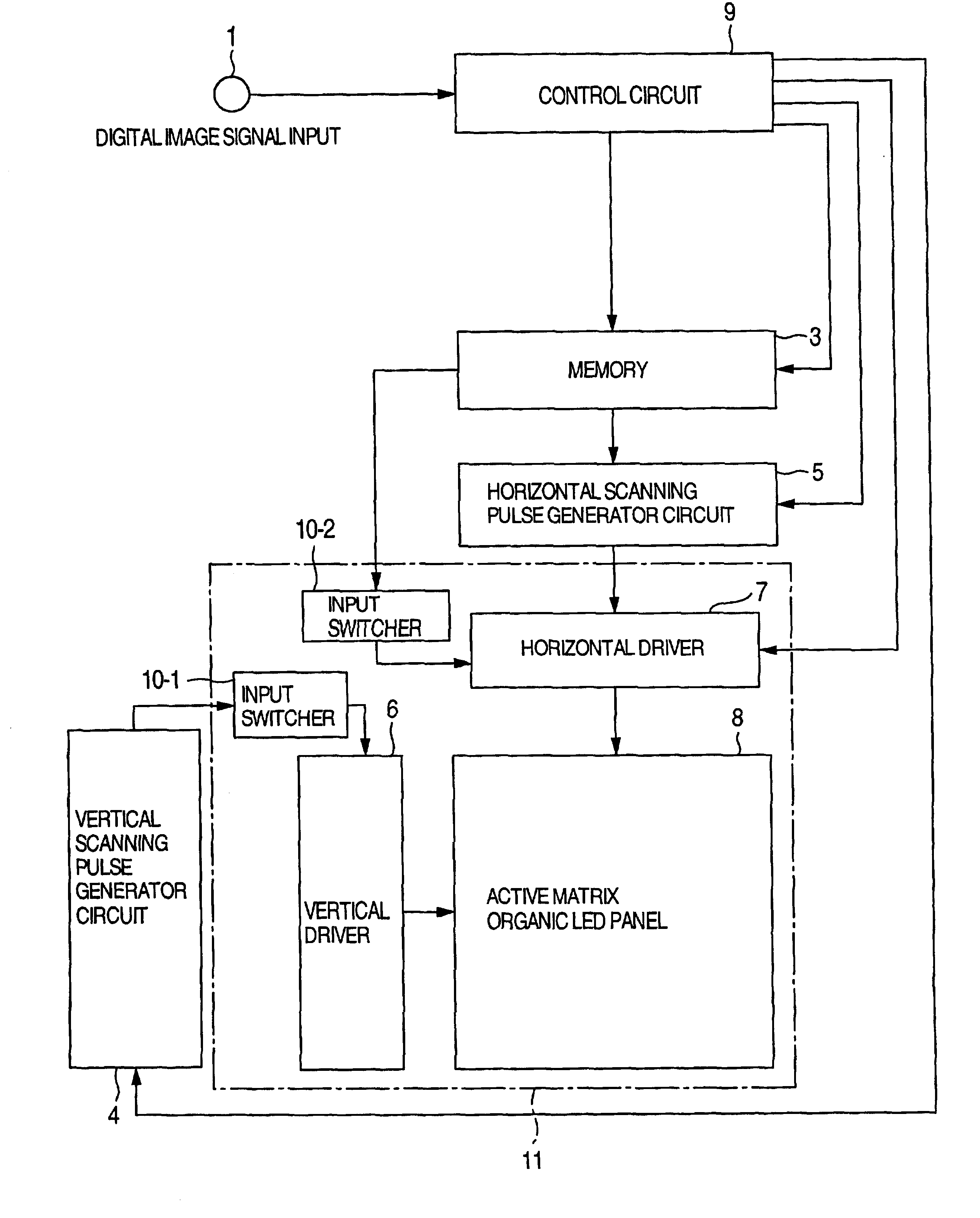
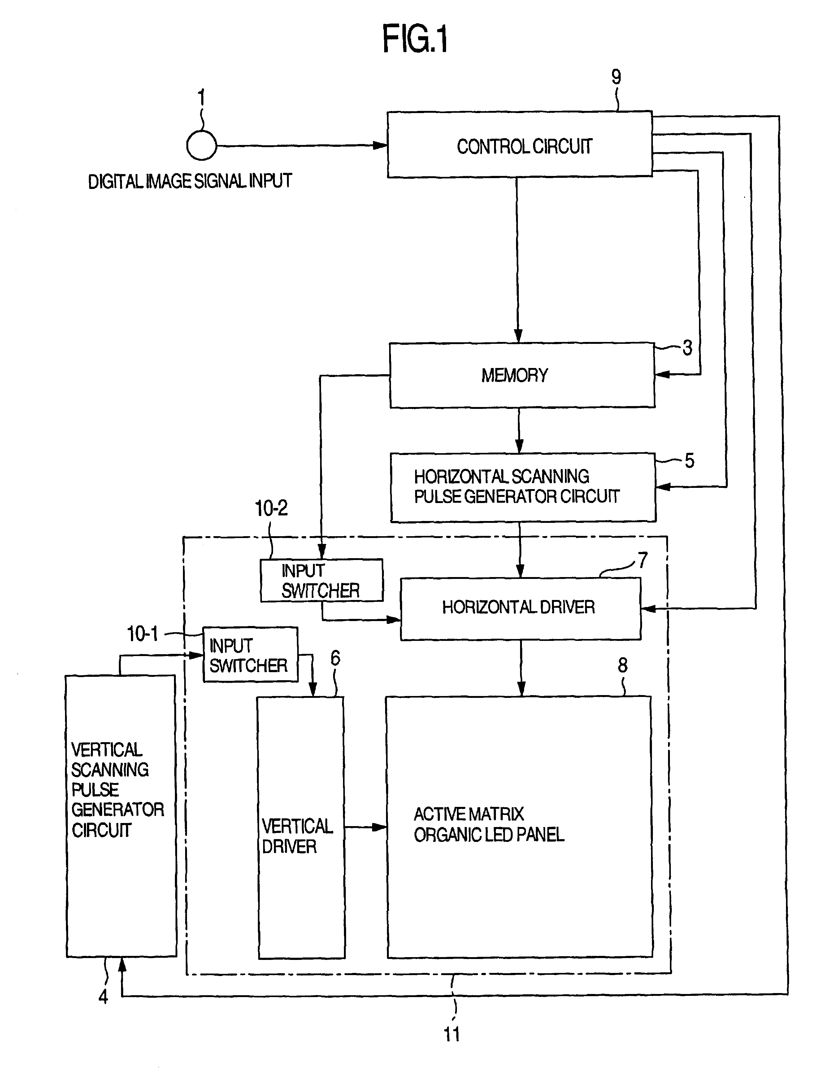
[0043]FIG. 1 is a block diagram of a major part of the first embodiment of an image display apparatus according to the present invention. The image display apparatus is constructed with an image signal input terminal 1, an A / D converter 2, a memory 3, a vertical scanning pulse generator circuit 4, a horizontal scanning pulse generator circuit 5, a vertical driver 6, a horizontal driver 7, an active matrix organic LED panel 8, a control circuit 9 and an input switchers 10-1 and 10-2. The vertical driver 6 having the input switcher 10-1 in an input portion thereof, the horizontal driver 7 having the input switcher 10-2 in an input portion thereof and the active matrix organic LED panel 8 as combined are generally referred to as a display portion 11. The display portion 11 has a construction of TFT drive with the same substrate.
[0044]Operation of each component shown in a form of block will be discussed hereinafter. The control circuit 9 generates various control signals in synchronism...
second embodiment
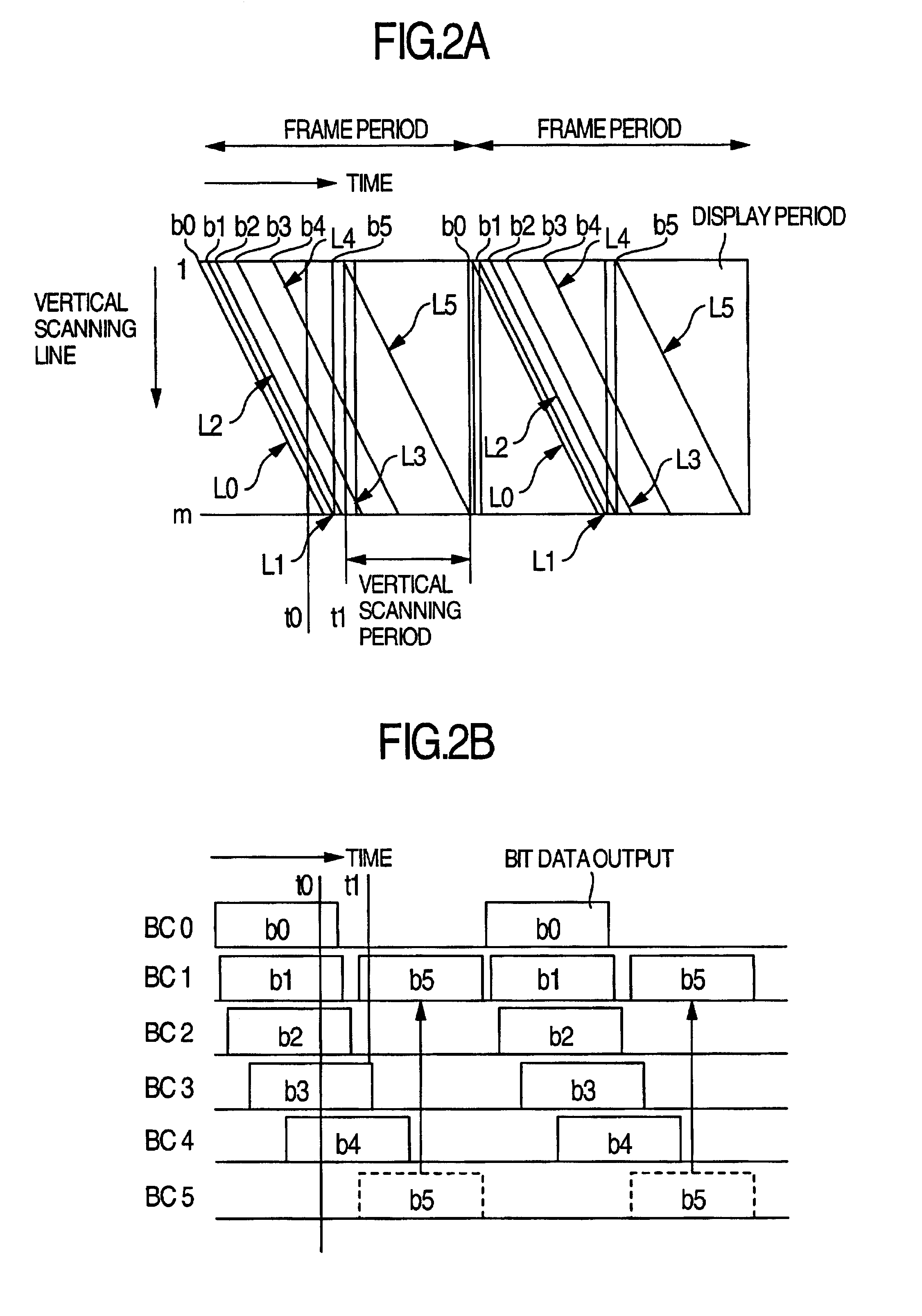
[0068]In the operation condition as illustrated in FIGS. 2A and 2B, observing at a certain timing, period to operate the sequence circuit and the logic operation circuit of the vertical drive circuit or line data latch circuit of the horizontal drive circuit corresponding to each bit data is data use period as shown in FIG. 2B.
[0069]In the shown example, at the time shown by vertically extending line, five bit data are used. Therefore, at least five sequence circuits and the logic operation circuits of the vertical drive circuit and line data latch circuits of the horizontal drive circuits are required. Namely, in the display apparatus for multiple gradation display with m (>n) bit digital data, if number of the sequence circuits and their logic operation circuits of the vertical drive circuit is n, the minimum value of n is equal to the maximum number of the bit data input at the same timing in the frame period.
[0070]On the other hand, the maximum value of the vertical scanning per...
third embodiment
[0078]As set forth above, by re-ordering data in the manner shown in the second embodiment, in case of 6-bit image data, the operation ratio is improved to be double in comparison with the case where order of data input of the first embodiment is used. However, operation ratio is still less than or equal to 50%. Procedure to further improve operation ratio will be discussed hereinafter.
[0079]As discussed in the second embodiment, for realizing the vertical driver and the horizontal driver with n stages of bit processing circuits for processing the m bits image data, the vertical scanning period Tvsc has to be less than or equal to the sums of the luminous periods of sequential n bits.
[0080]Here, when the sum of the luminous periods of sequential n bits is tlbn, tlbn means a period from inputting of certain data to the sequence circuit of the vertical drive circuit or the line data latch circuit of the horizontal drive circuit to input of the next data to the same sequence circuit of...
PUM
 Abstract
Description
Claims
Application Information