Optical-interference type reflective panel and method for making the same

a reflective panel and optical interference technology, applied in the direction of optical elements, instruments, coatings, etc., can solve the problems of affecting the appearance of the panel, so as to achieve the effect of simplifying the manufacturing process of the panel

Active Publication Date: 2006-02-14
SNAPTRACK
View PDF3 Cites 183 Cited by
  • Summary
  • Abstract
  • Description
  • Claims
  • Application Information

AI Technical Summary

Benefits of technology

[0014]One objective of the present invention is to provide an optical-interference type reflective panel and a method for making the same, wherein the manufacturing procedure for the panel is simplified.
[0019]Because said supporting layers forming step is prior to the first conductive optical film stacks, a precise back-side exposing step is not necessary so that the fabricating procedure of the panel is simplified.

Problems solved by technology

Inside the LCD device, the back light module consumes the most power of all the elements.
Even though these thin films are pervious to light, a partial amount of light may be blocked or lost while light passes through these films.
However, the fabricating process of the conventional panel is quite complex.
Thus, the entire panel manufacturing process is particularly complex.

Method used


Image

  • Optical-interference type reflective panel and method for making the same
  • Optical-interference type reflective panel and method for making the same
  • Optical-interference type reflective panel and method for making the same

Examples


Embodiment Construction

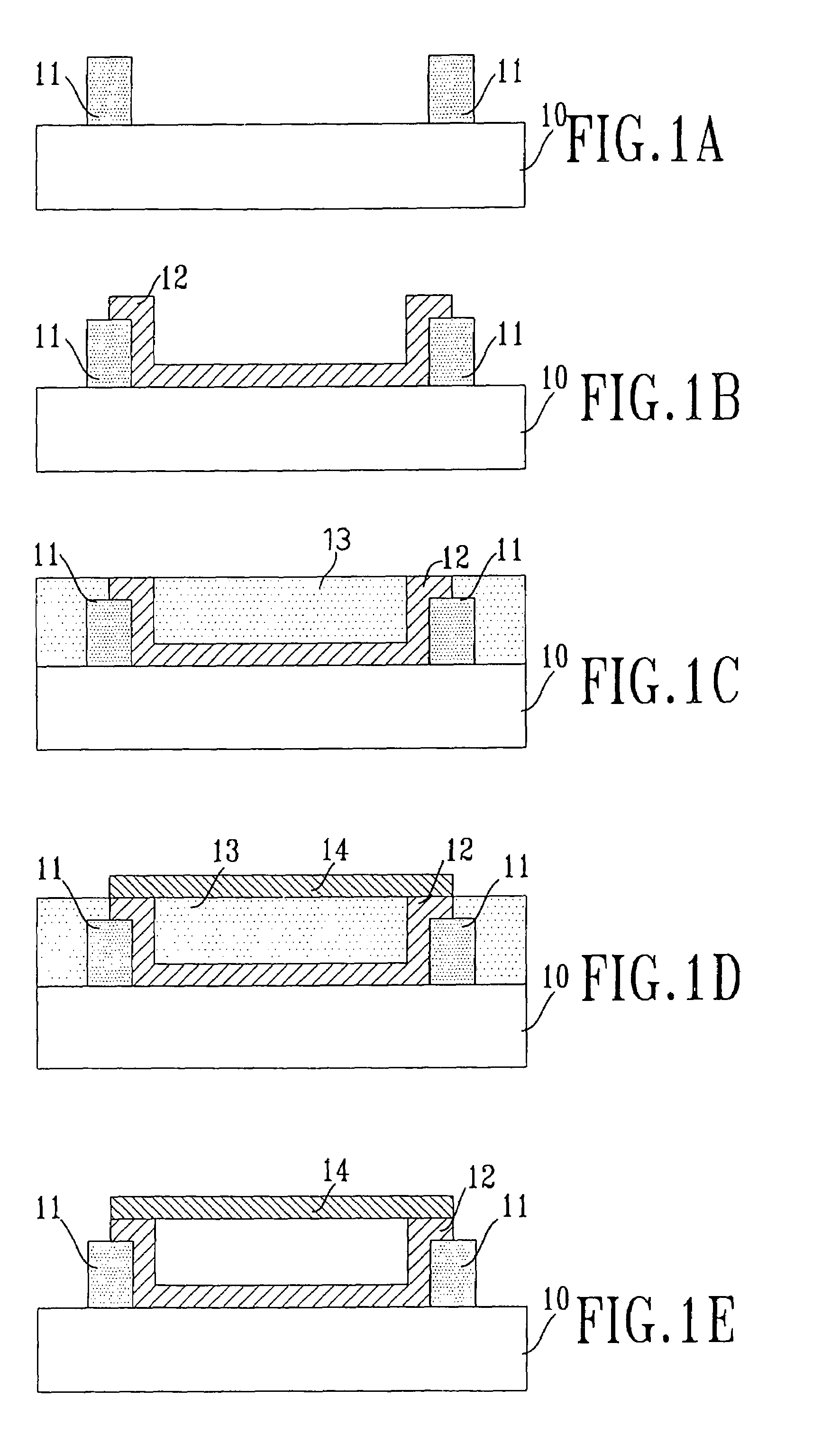
[0025]With reference to FIGS. 1A to 1E, a manufacturing process of an optical interference panel in accordance with the present invention is disclosed. The process includes the following steps.

[0026]As shown in FIG. 1A, a plurality of the supporting layers (11) is formed on a substrate (10) that is composed of glass or macromolecule material.

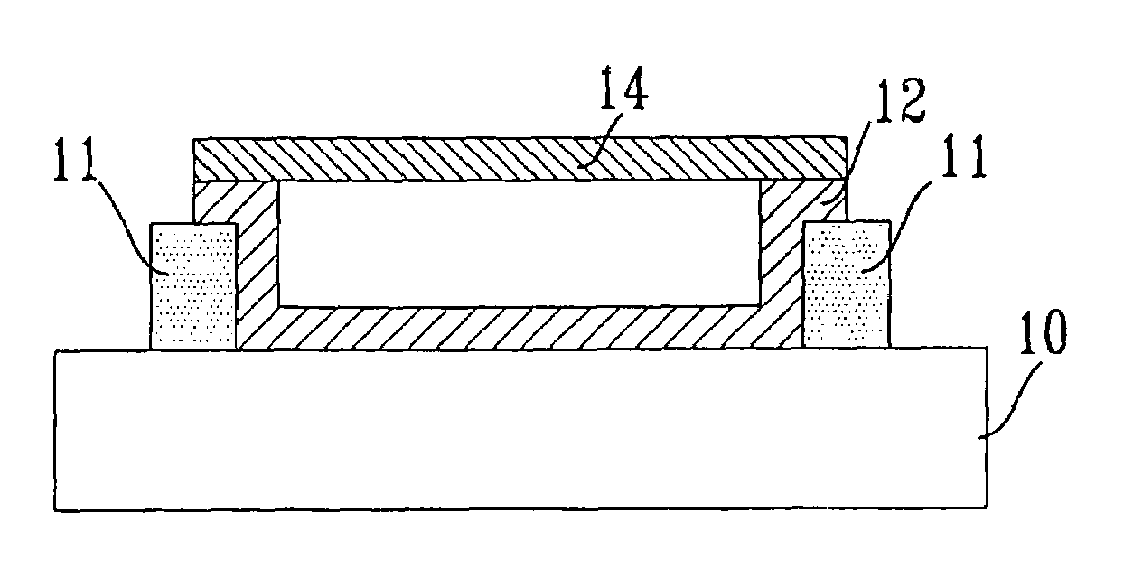
[0027]In FIG. 1B, a first conductive optical film stack (12) is then formed on the substrate (10) and between adjacent supporting layers (11), wherein the first conductive optical film stack (12) also covers a partial surface of the adjacent supporting layers (11).

[0028]With reference to FIG. 1C, a spacing layer (13), which is also called a sacrificing layer, is applied on the entire substrate (10) and flattened.

[0029]With reference to FIG. 1D, a second conductive optical film (14) is formed on the spacing layer (13) and between the adjacent supporting layers (11).

[0030]In FIG. 1E, the spacing layer (12) is removed from the substrate (10), where...


PUM

PropertyMeasurementUnit
conductiveaaaaaaaaaa
transparentaaaaaaaaaa
sizeaaaaaaaaaa

Abstract

An optical-interference type reflective panel and a method for making the same are disclosed, wherein the display panel has a substrate on which multiple supporting layers are firstly formed. Then, a plurality of first conductive optical film stacks, spacing layers and multiple second conductive optical film stacks are sequentially formed on the substrate. Finally, once the spacing layers are removed, optical-interference regulators are formed. Since said supporting layers forming step is prior to the first conductive optical film stacks, a precise back-side exposing step is not necessary so that the making procedure of the panel is simplified.

Description

BACKGROUND OF THE INVENTION[0001]1. Field of the Invention[0002]The present invention relates to an optical-interference type reflective panel and a method for making the same, and more particularly to a reflective panel for which a supporting layer forming step is prior to a first conductive optical film stack forming step so as to simplify the manufacturing process of the reflective panel.[0003]2. Description of Related Art[0004]In order to minimize the bulky size of a computer display, the flat display was developed to replace the conventional CRT display. For example, the most well known flat display is the LCD. In recent years, different kinds of LCDs have been developed by display manufacturers. Most of these manufacturers are dedicated as far as possible to reduce the power consumption of the display so that the LCD will become more suitable for portable electronic products such as cell phones, PDAs and E-books.[0005]Inside the LCD device, the back light module consumes the m...

Claims


Application Information

Patent Timeline
Patent Type & Authority Patents(United States)
IPC IPC(8): G02B1/10G02B26/02B32B7/02B81B3/00B81C1/00G02B5/28
CPCG02B26/001G02B5/288B32B7/023
Inventor LIN, WEN-JIANTSAI, HSIUNG-KUANG
Owner SNAPTRACK
Why Eureka
Try Eureka