Supercharge Your Innovation With Domain-Expert AI Agents!

Process for measuring bond-line thickness

a technology of bond-line thickness and thickness measurement, which is applied in the direction of individual semiconductor device testing, semiconductor/solid-state device testing/measurement, instruments, etc., can solve the problems of difficult to discern the exact interface, both destructive and time-consuming, and heat dissipation of active semiconductor devices

Inactive Publication Date: 2010-07-27
INT BUSINESS MASCH CORP
View PDF9 Cites 13 Cited by
  • Summary
  • Abstract
  • Description
  • Claims
  • Application Information

AI Technical Summary

Problems solved by technology

Heat dissipation from active semiconductor devices has become a major technical challenge in achieving continued increases in performance and function.
The most common method is cross-sectioning which is both destructive and time consuming providing only a few points of measurement over the chip area.
However, because of the large difference in the hardness of materials that include silicon, copper and polymers, materials are torn out or smeared during grinding and polishing therefore making it difficult to discern the exact interface.
It takes several days to complete cross-sectional analysis on a few modules, so this method is viable for development work and failure analysis but not for real-time process characterization or line monitoring.
For processes that require pressure during cure, this method could only be used after cure as laser scanning of the heat spreader is not possible in a force loaded cure fixture.
A second z-scope method that is destructive entails removing the heat spreader after cure.
Thus the bond line between the chip and heat spreader is not uniform.
Measuring the bond line over the entire chip area is not practical via cross sectioning.
Thus, it is becoming even more difficult to make accurate measurement of the bond line.

Method used


Image

  • Process for measuring bond-line thickness
  • Process for measuring bond-line thickness
  • Process for measuring bond-line thickness

Examples


Embodiment Construction

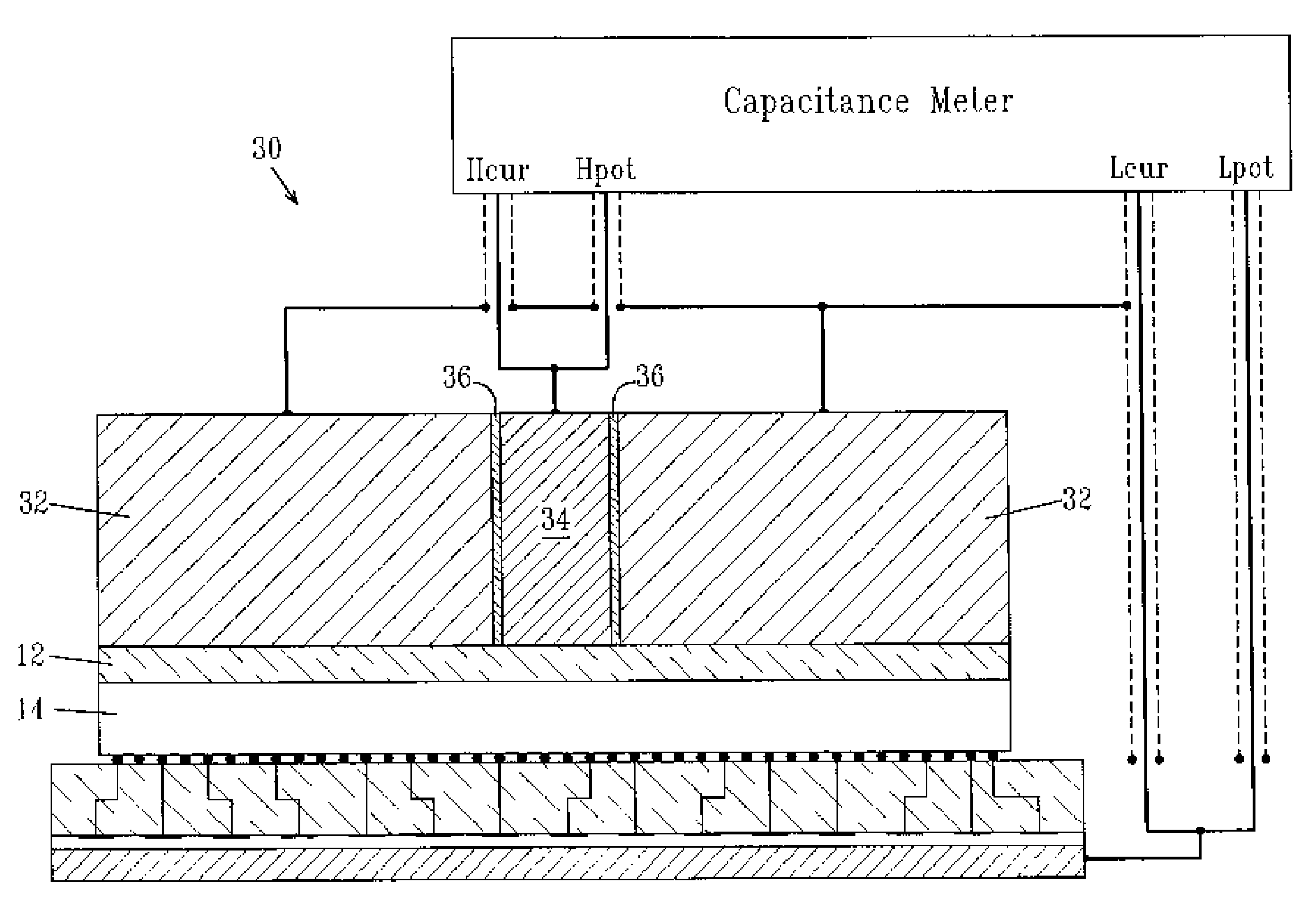
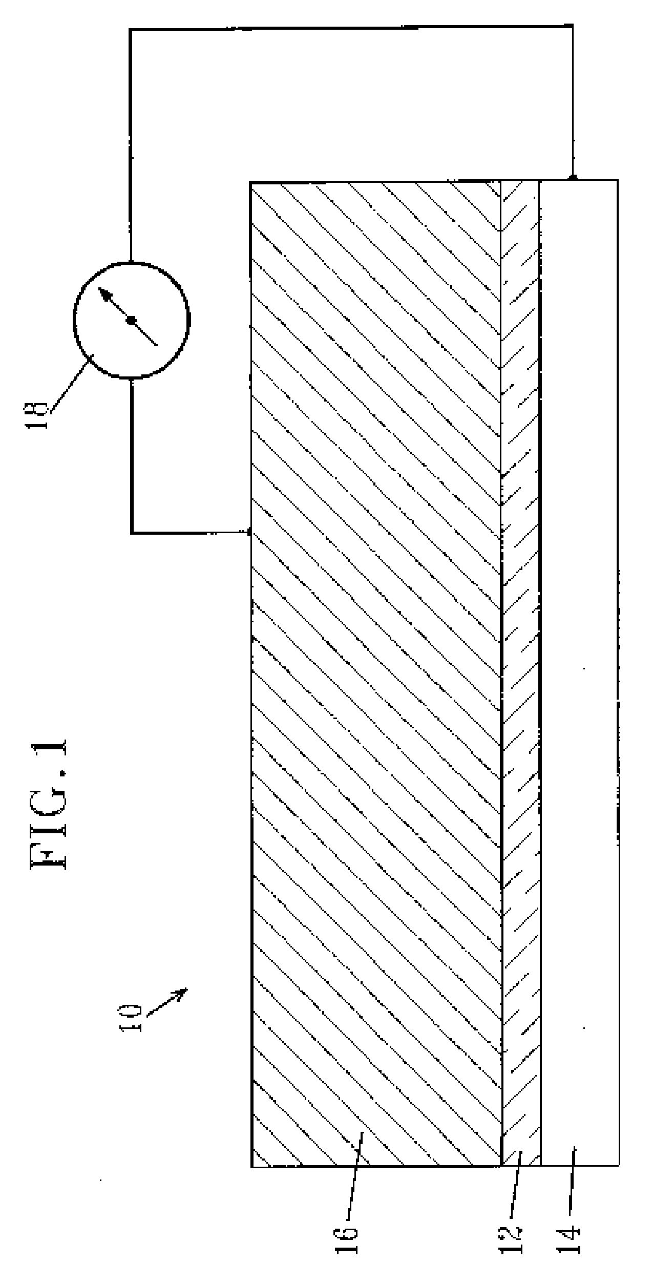
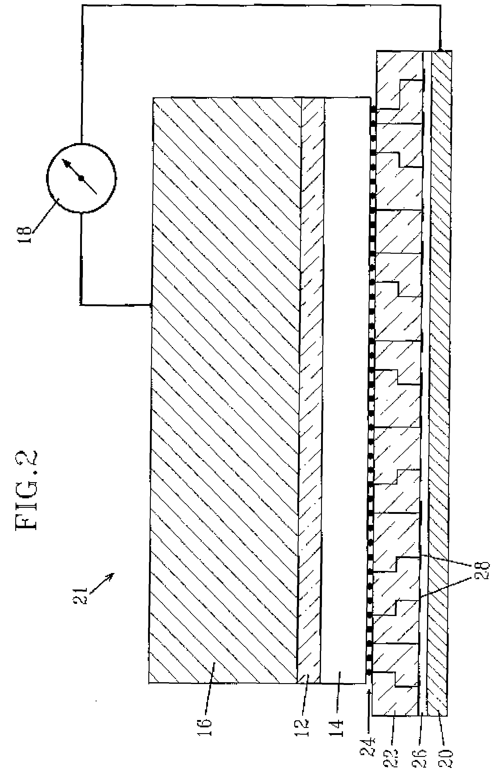
[0017]The invention is directed to a process for measuring the thickness of an insulating material. The process includes providing a device used to measure capacitance, and electrically connecting the capacitance measuring device to a heat sink and an electrical, heat-generating component. The insulating material is disposed between the heat sink and the heat-generating component. The thickness of the insulating material is determined by measuring the capacitance of the insulating material according to the formula;

B=∈r∈oA / C,

[0018]where B is the thickness of the insulating material, C is the capacitance, A is the area of the heat generating component, ∈o is the permittivity of free space and ∈r is the relative dielectric constant of the insulating material.

[0019]In one embodiment, the insulating material is a dielectric material and the heat-generating component is a semiconductor chip.

[0020]The process can be used to measure the bond-line thickness of a semiconductor package. In su...


PUM


Abstract

A process for measuring the thickness of an insulating material. The process includes providing a device used to measure capacitance, and electrically connecting the capacitance measuring device to a heat sink and an electrical, heat-generating component. The thickness of the insulating material is determined by measuring the capacitance of the insulating material according to the formula;B=∈r∈oA / C, where B is the thickness of the insulating material, C is the capacitance, A is the area of the heat generating component, ∈o is the permittivity of free space and ∈r is the relative dielectric constant of the insulating material.

Description

FIELD OF THE INVENTION[0001]The invention is related to a process for measuring the thickness of an insulating material. The invention is also related to an apparatus and package structure that provides for capacitance measurements so that the thickness of the insulating material can be determined.BACKGROUND OF THE INVENTION[0002]Heat dissipation from active semiconductor devices has become a major technical challenge in achieving continued increases in performance and function. The thermal resistance between the backside of a flip chip and the heat spreader attached to it decreases as the bulk thermal conductivity of the thermal interface material (TIM) increases and as the bond line thickness decreases. Therefore, accurate measurement of the bond line over the entire chip area is essential to design and predict the thermal resistance. Conventional methods to measure bond line include cross-sectioning; laser profiling before and after lid attach; and lid removal after cure combined...

Claims


Application Information

Patent Timeline
Patent Type & Authority Patents(United States)
IPC IPC(8): G01R27/26G01R31/26
CPCG01B7/08
Inventor GAYNES, MICHAEL A.YARMCHUK, EDWARD J.
Owner INT BUSINESS MASCH CORP
Features
  • R&D
  • Intellectual Property
  • Life Sciences
  • Materials
  • Tech Scout
  • Unparalleled Data Quality
  • Higher Quality Content
  • 60% Fewer Hallucinations
Learn More