
Internal voltage generating circuit
a voltage generation circuit and voltage generation technology, applied in pulse generators, instruments, pulse techniques, etc., can solve the problems of poor sensitivity, difficult to stably operate the mos transistor, severe operation conditions of the mos transistor, etc., and achieve the effect of sufficient controllability and stability
- Summary
- Abstract
- Description
- Claims
- Application Information
AI Technical Summary
Benefits of technology
Problems solved by technology
Method used
Image



Examples
embodiment 1
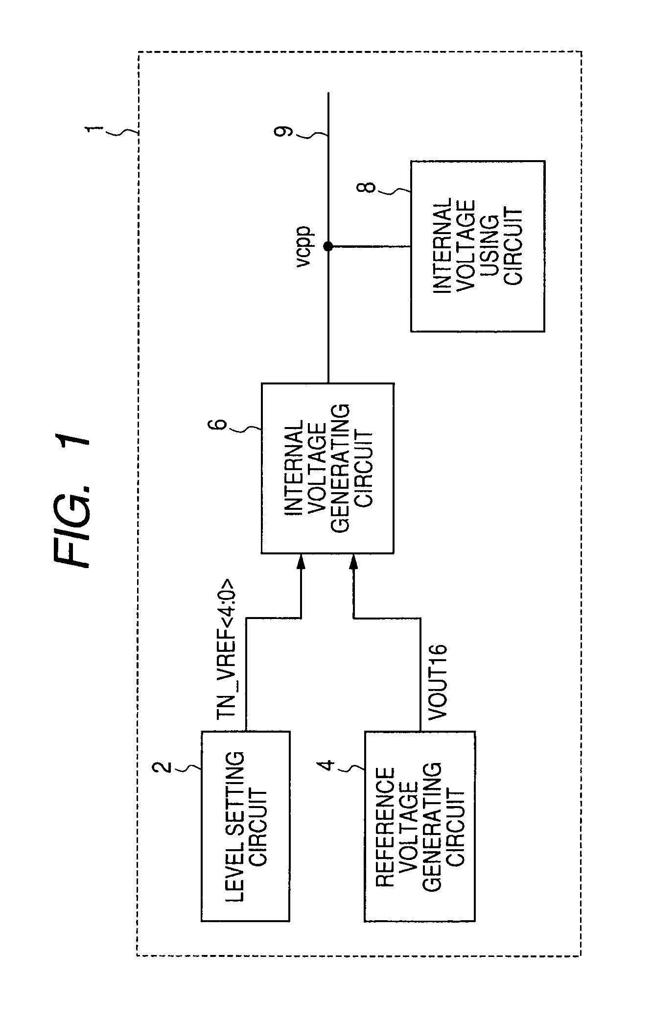
[0033]FIG. 1 schematically illustrates an entire configuration of the semiconductor integrated circuit device including an internal voltage generating circuit, according to Embodiment 1 of the present invention. As illustrated in FIG. 1, the semiconductor integrated circuit device 1 comprises a level setting circuit 2 which generates a basic voltage code (digital value) TN_VREF to specify a desired voltage level of an internal voltage VCPP, a reference voltage generating circuit 4 which generates a reference voltage VOUT16 independent of temperature, and an internal voltage generating circuit 6 which generates an internal voltage VCPP according to the basic voltage code TN_VREF and the reference voltage VOUT16. The internal voltage generating circuit 6 generates the internal voltage VCPP on an internal power supply line 9, and the internal voltage VCPP is used by an internal voltage using circuit 8.
[0034]The level setting circuit 2 generates the basic voltage code TN_VREF which s...
embodiment 2
[0098]FIG. 9 schematically illustrates a configuration of the principal part of an internal voltage generating circuit according to Embodiment 2 of the present invention. In the configuration illustrated in FIG. 9, a shifter 60 is provided between the A / D conversion circuit 12 and the adder circuit 14. The present shifter 60 executes a right shift operation by one bit or a left shift operation by one bit to the digital standard voltage code TN_VRFAD outputted by the A / D conversion circuit 12. By the operation, multiplication or division of the output code TN_VRFAD of the A / D conversion circuit 12 is performed. A shift code SHAD from the shifter 60 is supplied to the adder circuit 14, and added with the basic voltage code TN_VREF .
[0099]The configuration of the temperature characteristic adding circuit 10, the A / D conversion circuit 12, and the adder circuit 14 of the internal voltage generating circuit illustrated in FIG. 9, and the components of the remaining internal voltage gen...
PUM
 Login to View More
Abstract
Description
Claims
Application Information
 Login to View More