
Data processing circuit with multiplexed memory
A memory circuit and data processing technology, applied in electrical digital data processing, instrumentation, climate sustainability, etc., can solve the problems of limited operation speed and high power consumption of equipment
Patent Information
- Authority / Receiving Office
- CN · China
- Current Assignee / Owner
- Publication Date
- 2009-04-29
- Estimated Expiration
- Not applicable · inactive patent
Smart Images
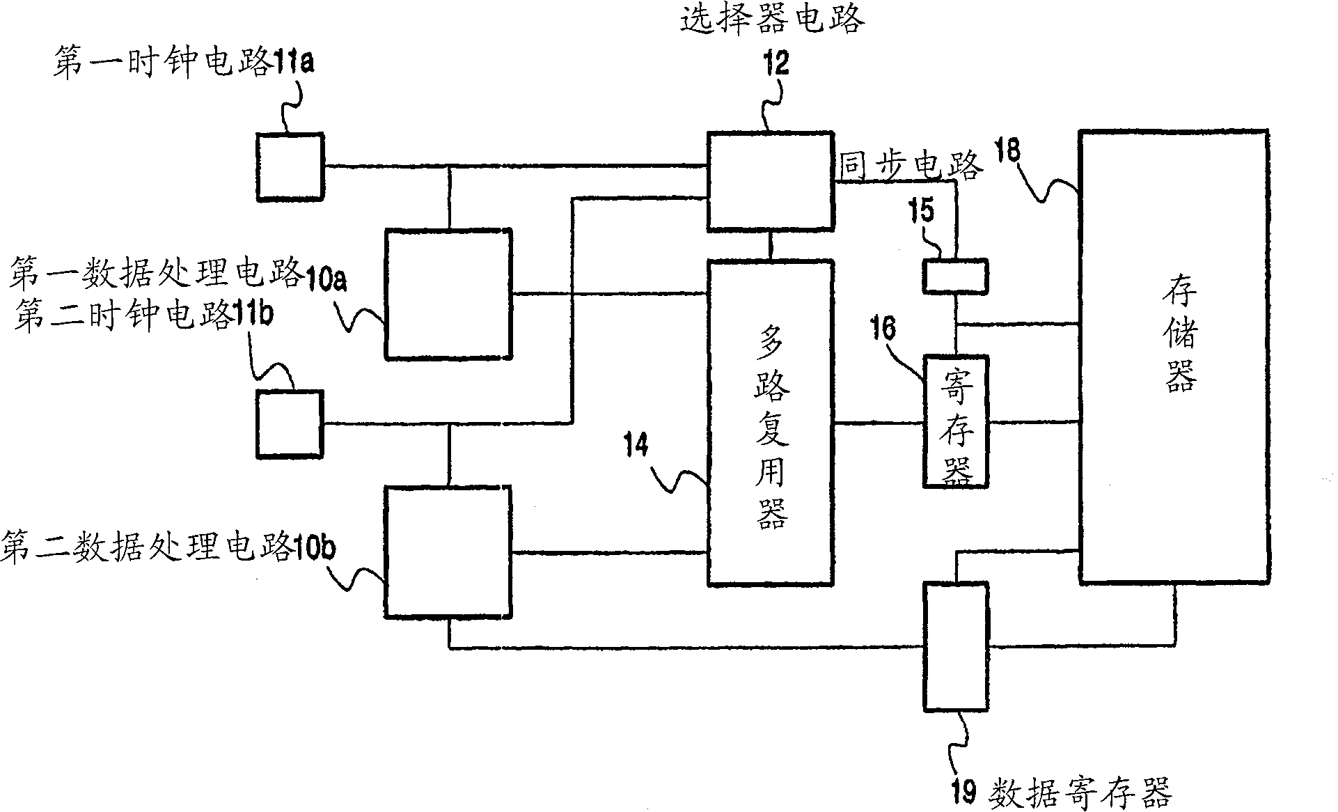
Figure 1 
Figure 2 
Figure 3
Abstract
Description
technical field
[0001] The invention relates to a device in which processing performed by different circuits accesses the same single-port memory circuit. Background technique
[0002] In theory, multi-port memory could be an ideal technology for enabling different circuits to independently access the same memory circuit. But in practice, actual multi-port memories are not popular because they contain a lot of system overhead compared with traditional single-port memories. Therefore, single-port memories are often used to implement pseudo-multiport memories.
[0003] From US Patent 5,706,482, published January 6, 1998, a device is known with a pseudo multi-port memory comprising a single-port memory for storing image data. Both the first circuit performing write processing and the second circuit performing read processing can access the memory. A FIFO write queue is provided between the memory port and the first circuit, and a FIFO read queue is provided between the memor...
Examples
Embodiment Construction
[0030] figure 1 A circuit is shown with a first data processing circuit 10a, a second data processing circuit 10b, a first clock circuit 11a, a second clock circuit 11b, a selector circuit 12, a multiplexer 14, a synchronization circuit 15 , register 16, memory 18 and data register 19. The first clock circuit 11 a is coupled to the first data processing circuit 10 a and the selector circuit 12 . The second clock circuit 11 b is coupled to the second data processing circuit 10 b and the selector circuit 12 . The first and second data processing circuits 10a, b have an access request information output coupled to an input of a multiplexer 14 which in turn has an output coupled to an input of a register 16 . Selector circuit 12 has a select output coupled to the control input of multiplexer 14 and a timing control output coupled to synchronization circuit 15 . Synchronization circuit 15 has a timing output coupled to register 16 and memory 18 . The data register 19 has an inp...