
Millimeter-wave four-polarized frequency scanning antenna
A frequency-scanning antenna and four-polarization technology, which is applied to antenna unit combinations with different polarization directions, slot antennas, circuits, etc., can solve the problems of circularly polarized beam scanning difficulties and achieve low loss, large power capacity, and mutual coupling effect
Patent Information
- Authority / Receiving Office
- CN · China
- Patent Type
- Patents(China)
- Current Assignee / Owner
- Publication Date
- 2012-07-25
Smart Images
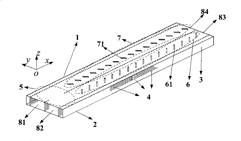
Figure 1 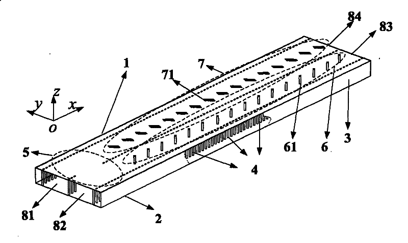
Figure 2
Abstract
Description
Technical field
[0001] The invention relates to a multi-polarization frequency scanning antenna that can be applied to the fields of millimeter wave wireless communication systems and radar detection, and belongs to the technical field of millimeter wave antenna design and manufacturing. Background technique
[0002] In various wireless communication and radar systems, the transmission and reception of information rely on antennas. With the rapid development of modern large-capacity, multi-functional, ultra-wideband integrated information systems, the number of information subsystems carried on the same platform has greatly increased, and the number of antennas required has also increased accordingly. This is in contradiction with the development trend of reducing the overall cost of the integrated information system, reducing the weight, reducing the platform radar cross section, and achieving good electromagnetic compatibility characteristics. Multi-polarization antennas can e...
Examples
Embodiment Construction
[0019] The millimeter wave quad-polarized frequency scanning antenna in the present invention includes an upper metal copper-clad surface 1, a lower metal copper-clad surface 2, a dielectric substrate 3, a metalized through hole 4, a substrate integrated waveguide 90° directional coupler 5, a base Chip integrated waveguide 16-slot 45° slot array leaky wave antenna 6, Substrate integrated waveguide 16-slot-45° slot array leaky wave antenna 7, input port 81, input port 82, input port 83, input port 84; copper-clad upper metal The surface 1 and the lower metal copper-clad surface 2 are respectively located on the front and back sides of the dielectric substrate 3, and the metallized through holes 4 pass through the dielectric substrate 3 to connect with the upper metal copper-clad surface 1 and the lower metal copper-clad surface 2 to form a base. Chip integrated waveguide 90° directional coupler 5. Substrate integrated waveguide 16-slot 45° slot array leaky wave antenna 6, Substra...