
Optical induction device with anti-static elements
An induction device and antistatic technology, applied in the field of optical induction devices, can solve problems such as the influence of the sensing accuracy of the optical induction device, and achieve the effect of eliminating adverse effects and improving the induction accuracy
Patent Information
- Authority / Receiving Office
- CN · China
- Current Assignee / Owner
- Publication Date
- 2011-08-17
- Estimated Expiration
- Not applicable · inactive patent
Smart Images
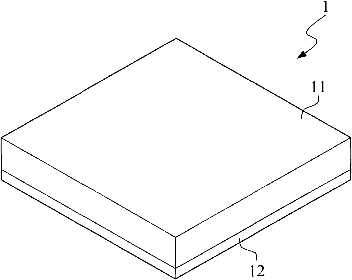
Figure 1 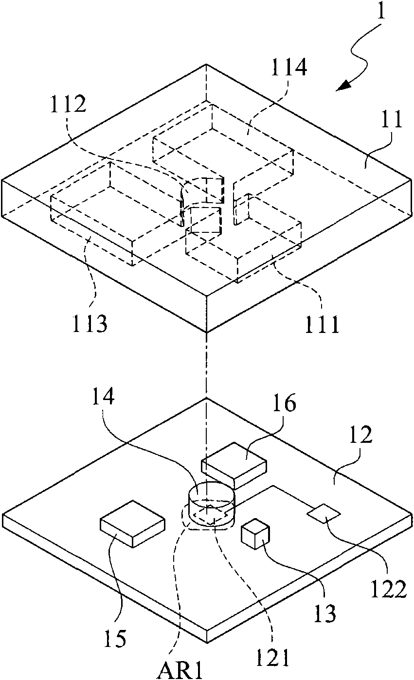
Figure 2 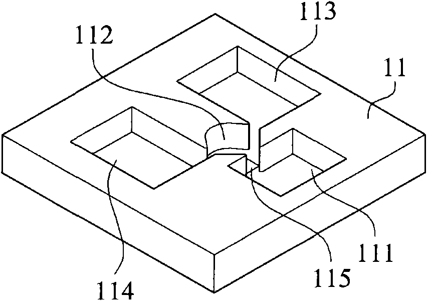
Figure 3
Abstract
Description
technical field
[0001] The invention relates to an optical sensing device, in particular to an optical sensing device with an antistatic element. Background technique
[0002] In daily life, in order to grasp the inclination angle or displacement of an object, various sensors are usually used, and these sensors usually include a horizontal displacement sensing function, a vertical displacement sensing function or an inclination angle sensing function. In practice, these sensors usually use many sensing technologies, such as optical sensing technology, acoustic wave sensing technology or electrical sensing technology. Among them, since the optical sensing technology has the advantages of fast sensing speed, it is gradually applied to the production of high-sensitivity sensing applications.
[0003] In most of the optical sensing devices produced by the prior art, a black body conditional space is enclosed in a casing, and a light emitting element, a shielding element and at ...
Examples
Embodiment Construction
[0043] Since the optical sensing device provided by the present invention can be widely used to sense the displacement or inclination of various objects to be sensed, especially for sensing the inclination of the object to be sensed, and the related combination implementations are too numerous to enumerate, so here No need to go into details one by one, but only two preferred embodiments are listed for specific description.
[0044] see Figure 1 to Figure 4 , figure 1 It is a perspective view showing the appearance of the optical sensing device in the first embodiment of the present invention; figure 2 for display when figure 1 The three-dimensional perspective schematic diagram of the middle shell separated from the circuit board; image 3 It is a schematic diagram showing the casing of the first embodiment of the present invention; Figure 4 It is a schematic diagram showing the working principle of the first embodiment of the present invention.
[0045] Such as Fig...