
Method of forming a fin field effect transistor
A fin-type field effect, transistor technology, applied in semiconductor devices, semiconductor/solid-state device manufacturing, electrical components, etc., can solve problems such as blocking source and drain surface epitaxial layers, short circuits, etc., to increase size, reduce resistance, The effect of increasing the drive current
Patent Information
- Authority / Receiving Office
- CN · China
- Patent Type
- Patents(China)
- Current Assignee / Owner
- Publication Date
- 2016-12-21
Smart Images
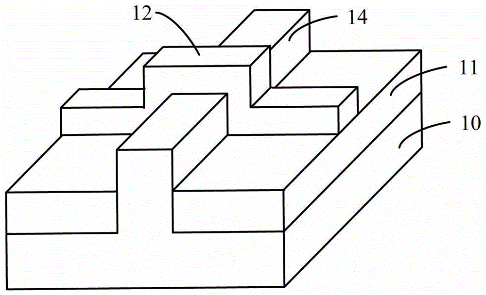
Figure 1 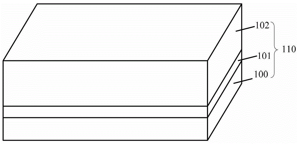
Figure 2 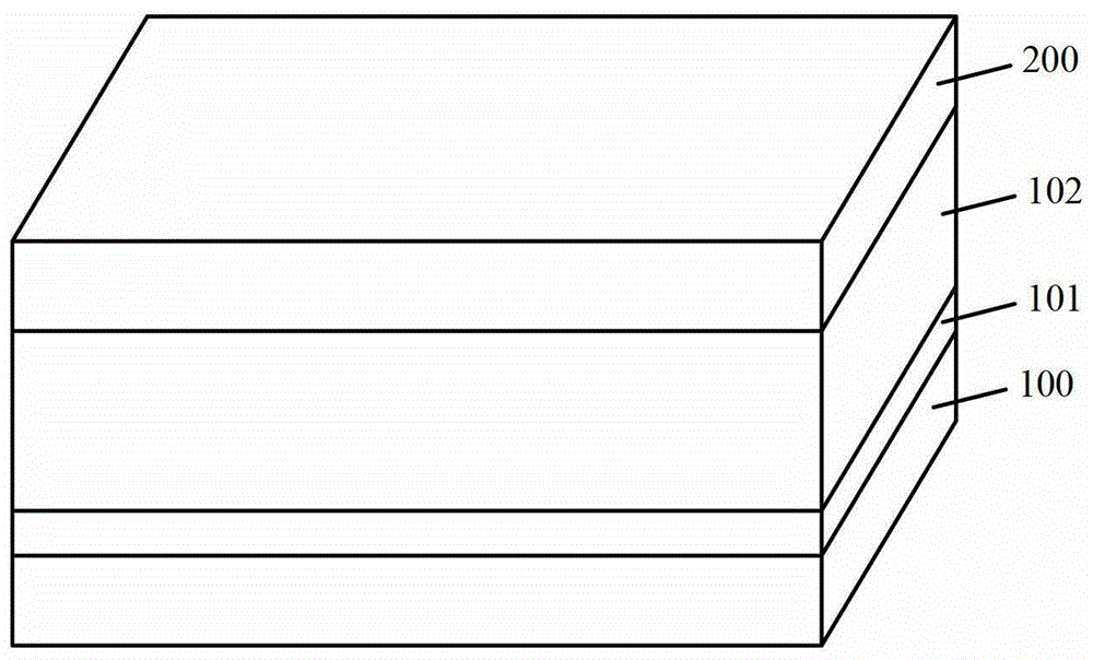
Figure 3
Abstract
Description
technical field
[0001] The invention relates to the technical field of semiconductors, in particular to a method for forming a fin field effect transistor. Background technique
[0002] With the continuous development of semiconductor process technology, the process node is gradually reduced, and the gate-last (gate-last) process has been widely used to obtain an ideal threshold voltage and improve device performance. However, when the feature size (CD, Critical Dimension) of the device is further reduced, even the field effect transistor manufactured by the gate-last process can no longer meet the demand for device performance, and multi-gate devices have gained widespread attention.
[0003] Fin field effect transistor (Fin FET) is a common multi-gate device, figure 1 A three-dimensional schematic diagram of a fin and a gate structure of a fin field effect transistor in the prior art is shown. Such as figure 1 As shown, it includes: a semiconductor substrate 10, a protr...
Examples
no. 1 example
[0035] Please refer to figure 2 , providing a semiconductor substrate 110 .
[0036] The material of the semiconductor substrate 110 includes semiconductor materials such as silicon, germanium, silicon germanium, gallium arsenide, etc., and may be a bulk material or a composite structure such as silicon-on-insulator or germanium-on-insulator. Those skilled in the art can select the type of the semiconductor substrate 110 according to the semiconductor devices formed on the semiconductor substrate 110 , so the type of the semiconductor substrate should not limit the protection scope of the present invention.
[0037] In this embodiment, the material of the semiconductor substrate 110 used is silicon-on-insulator, including a silicon substrate layer 100 , a middle silicon oxide layer 101 and a single crystal silicon top layer 102 .
[0038] Please refer to image 3 , forming a hard mask material layer 200 on the surface of the semiconductor substrate 110 .
[0039] Specifica...
no. 2 example
[0070] This embodiment also provides another method for forming a FinFET.
[0071] Please refer to Figure 17 , using the same method as the first embodiment, after forming the hard mask layer 201 on the surface of the substrate, etching the semiconductor substrate to form the pre-processing fins 500 .
[0072] Please refer to Figure 18 , growing an epitaxial layer 501 on the sidewall of the pre-processing fin, the pre-processing fin 500 and the epitaxial layer 501 on both sides thereof form a fin 510 .
[0073] Specifically, in this embodiment, the material of the epitaxial layer 501 is silicon. In other embodiments of the present invention, the material of the epitaxial layer 501 may also be silicon germanium or silicon carbide. The epitaxial layer 501 can be a single-layer silicon, silicon germanium or silicon carbide structure, or a multi-layer structure formed of multiple layers of different materials. For example, a layer of germanium is first grown on the sidewall o...