
Power source ground network and wire arrangement method thereof
A wiring method and power line technology, which is applied in the direction of circuits, electrical components, and electric solid devices, can solve problems such as the drop in power supply voltage of reaching devices, the drop in chip frequency, and the impact on chip performance, so as to reduce the voltage drop and increase the size of the grid Density, effect of transmission path shortening
Patent Information
- Authority / Receiving Office
- CN · China
- Patent Type
- Applications(China)
- Current Assignee / Owner
- Publication Date
- 2014-12-24
Smart Images
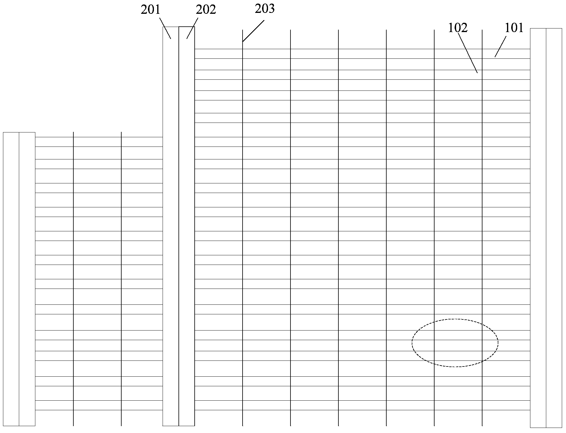
Figure 1 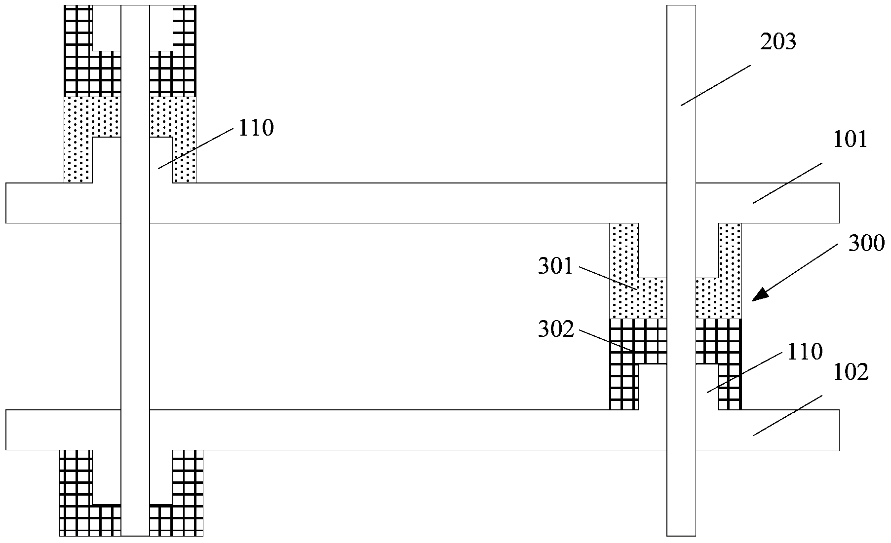
Figure 2 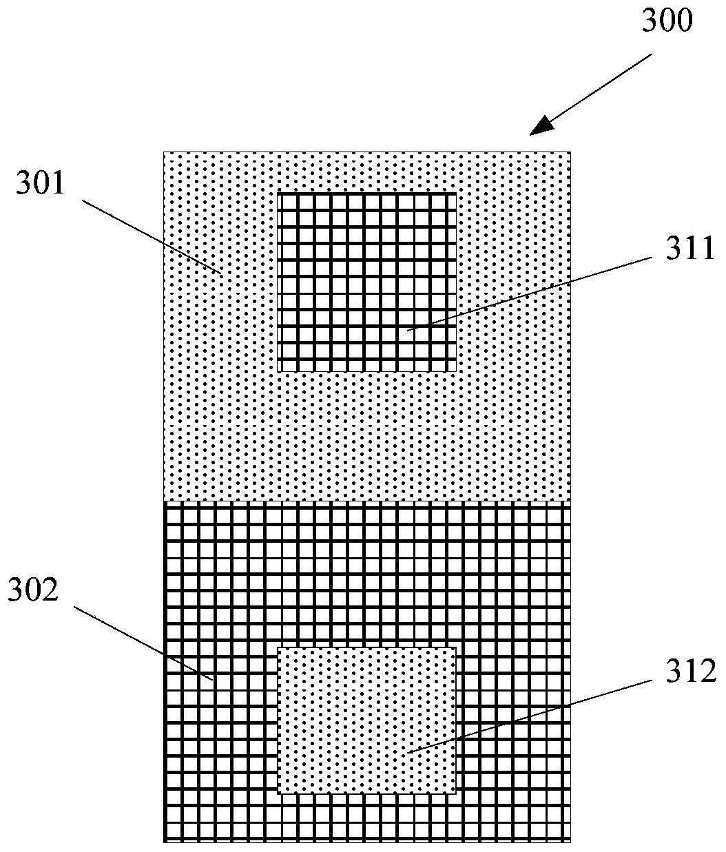
Figure 3
Abstract
Description
technical field
[0001] The invention relates to the technical field of semiconductors, in particular to a power ground network and a wiring method thereof. Background technique
[0002] With the advancement of semiconductor technology, the traditional two-dimensional chip design will encounter some bottlenecks. The three-dimensional integrated circuit introduces through-silicon metal contact holes (Through-Silicon-Via, TSV) in the vertical direction. Chips are stacked in the vertical direction, which can reduce the length of interconnection lines on the chip, increase the number of input / output ports between chips, and improve data transmission bandwidth. In addition, three-dimensional integrated circuits also have the advantages of supporting heterogeneous integration and smaller external dimensions, and gradually become the development direction of the next generation of integrated circuits.
[0003] The three-dimensional integrated circuit uses the power supply network t...
Examples
Embodiment Construction
[0040] As mentioned in the background art, the problem of voltage drop (IR-Drop) in the power-ground network becomes more and more significant, which seriously affects the performance of the chip.
[0041] The study found that the voltage drop of the power ground network can be reduced by widening the width of the power line and ground line in the power ground network. However, as the process becomes smaller and smaller, the chip size is also shrinking, and the wiring resources are limited. There are certain limitations in increasing the width of the power line and ground line, which may affect the layout of other devices.
[0042] Another way to reduce the voltage drop of the power supply network is to increase the number of decoupling capacitors on the chip to limit the voltage drop. However, more decoupling capacitors will occupy a larger chip area, thereby increasing the overall area of the chip. Thereby reducing the integration level of the chip and increasing the cost ...