
A kind of oled device and its preparation method, oled display panel
A technology for devices and light-emitting layers, which is applied in the field of OLED devices and their preparation, and OLED display panels, and can solve problems such as poor color stability and large changes in color coordinates of OLED devices
Patent Information
- Authority / Receiving Office
- CN · China
- Current Assignee / Owner
- Publication Date
- 2018-07-06
- Estimated Expiration
- Not applicable · inactive patent
Smart Images
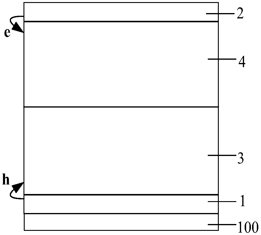
Figure 1 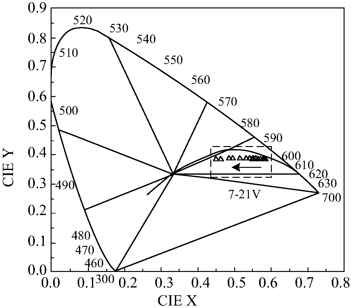
Figure 2 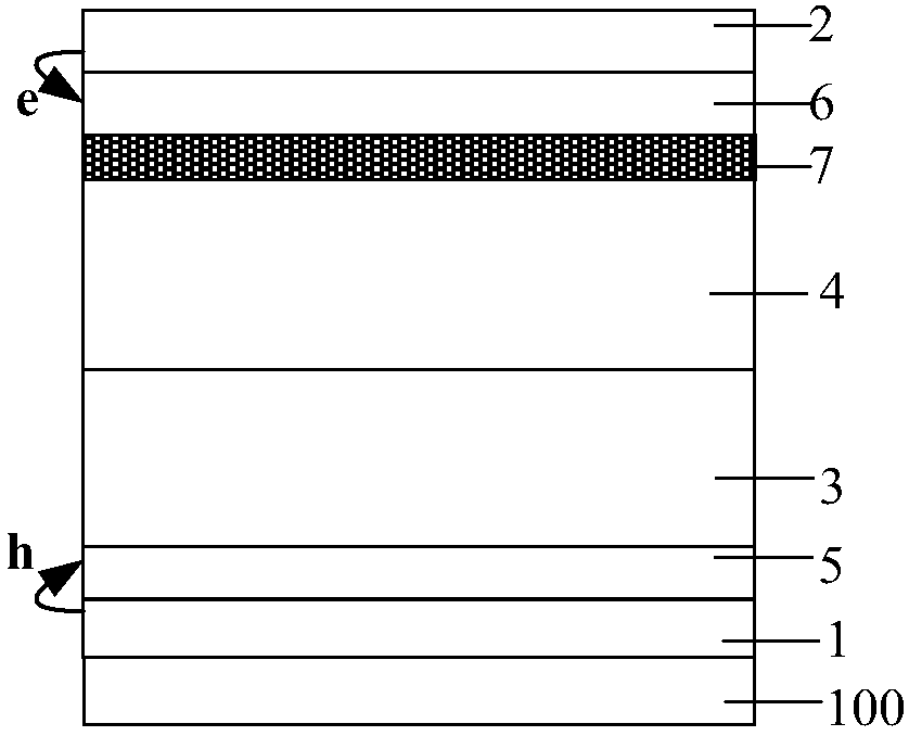
Figure 3
Abstract
Description
technical field
[0001] The invention relates to the field of display technology, in particular to an OLED device, a preparation method thereof, and an OLED display panel. Background technique
[0002] Organic Light Emitting Diode (OLED) is an organic thin-film electroluminescent device, which has the advantages of simple preparation process, low cost, easy formation of flexible structure, and wide viewing angle. Therefore, the use of organic electroluminescence Diode display technology has become an important display technology.
[0003] Such as figure 1 As shown, the white light OLED device in the prior art includes: an anode 1 and a cathode 2 arranged on a substrate 100, and a first light-emitting layer 3 and a second light-emitting layer located between the anode 1 and the cathode 2 4. The principle of light emission is: holes (h) injected from the anode 1 and electrons (e) injected from the cathode 2 combine in the light-emitting layer to form excitons, which excite t...
Examples
Embodiment Construction
[0030] The following will clearly and completely describe the technical solutions in the embodiments of the present invention with reference to the accompanying drawings in the embodiments of the present invention. Obviously, the described embodiments are only some, not all, embodiments of the present invention. Based on the embodiments of the present invention, all other embodiments obtained by persons of ordinary skill in the art without making creative efforts belong to the protection scope of the present invention.
[0031] An embodiment of the present invention provides an OLED device, such as Figure 3-5 As shown, the OLED device includes an anode 1 disposed on a substrate 100, a cathode 2, a hole transport layer 5 and an electron transport layer 6 disposed between the anode 1 and the cathode 2, and an electrode disposed between the hole transport layer 5 and the At least two light-emitting layers between the electron transport layer 6, wherein the above-mentioned at lea...