
Circuit arrangement and method for controlling a junction field effect transistor
A field effect transistor and circuit arrangement technology, applied in the direction of using electrical devices, thermometers using electrical/magnetic components directly sensitive to heat, using electromagnetic means, etc., can solve problems such as being unsuitable for actual operation, and achieve the effect of avoiding interruptions
Patent Information
- Authority / Receiving Office
- CN · China
- Patent Type
- Patents(China)
- Current Assignee / Owner
- Publication Date
- 2020-01-21
Smart Images
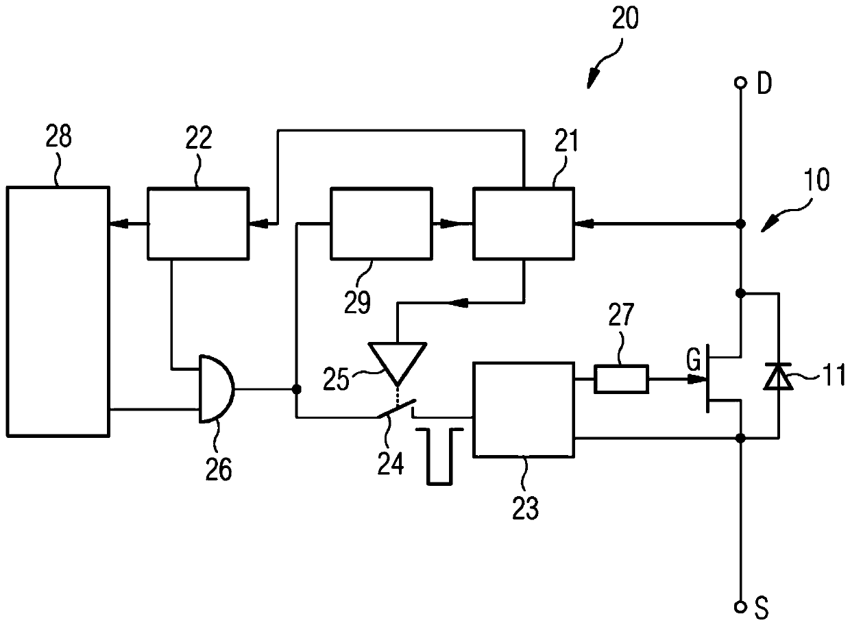
Figure 1 
Figure 2 
Figure 3
Abstract
Description
technical field
[0001] The invention relates to a circuit arrangement and a method for controlling a semiconductor switching element in the form of a junction field effect transistor comprising a first main connection and a second main connection and forming a channel therebetween. Background technique
[0002] Semiconductor switching elements are used, for example, as power switching elements. Therein lies the need to monitor the temperature of the semiconductor switching element so that the semiconductor switching element and the module comprising the semiconductor switching element (also referred to as a system) as a whole can function reliably. In the event of excessive temperatures, the circuit arrangement controlling the semiconductor switching elements must ensure reliable switching off.
[0003] For this purpose, for example, an external temperature sensor such as an NTC temperature sensor is used. It is arranged, for example, on a carrier plate in a module contain...
Examples
Embodiment Construction
[0024] figure 1 An exemplary embodiment of a circuit arrangement 20 according to the invention for controlling a junction field effect transistor 10 is shown. The junction field effect transistor 10 may be, for example, a silicon carbide field effect transistor (SiC-JFET). The JFET 10 comprises a control connection G (gate) and a first main connection D (drain) and a second main connection S (source). A channel is formed between the first main terminal D and the second main terminal S, and when the JFET 10 is switched on, current can flow through the channel. The body diode present between the second main connection (S) and the first main connection (D) is indicated with 11 .
[0025] The control connection G, for example a junction field effect transistor, is connected to a p-conduction region arranged in an n-conduction (substrate) material. The p-type conduction region and the n-type conduction material of the JFET form a p-n diode. A Junction Field Effect Transistor (J...