
Pixel circuit and driving method thereof, display panel and display device
A technology for pixel circuits and driving transistors, which is applied in the fields of pixel circuits, display panels and display devices, and can solve problems such as uneven display screens, achieve the effects of optimizing the selection range, stabilizing pixel circuits, and reducing energy consumption
Patent Information
- Authority / Receiving Office
- CN · China
- Patent Type
- Applications(China)
- Current Assignee / Owner
- Publication Date
- 2017-11-17
Smart Images
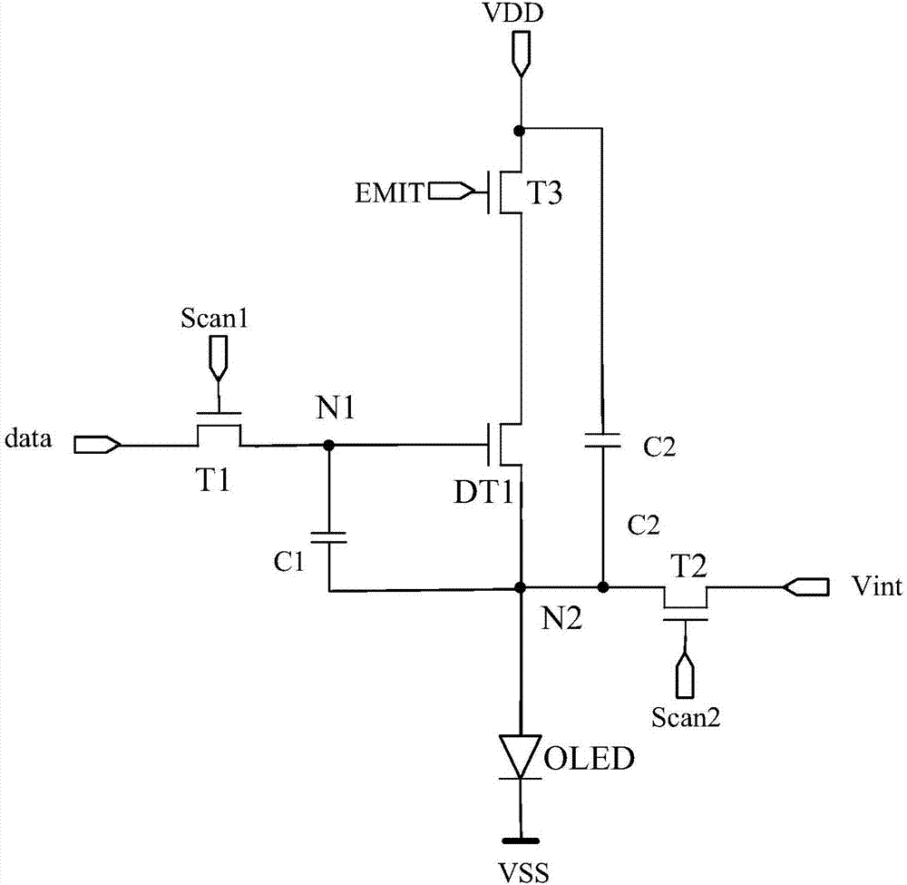
Figure 1 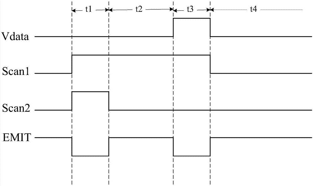
Figure 2 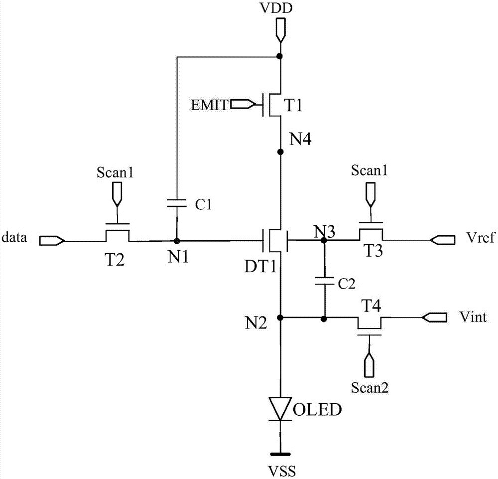
Figure 3
Abstract
Description
technical field
[0001] The invention relates to the field of display technology, in particular to a pixel circuit, a driving method thereof, a display panel and a display device. Background technique
[0002] Organic Light Emitting Diode (OLED) is one of the hot spots in the field of display research today. Compared with Liquid Crystal Display (LCD), OLED has low energy consumption, low production cost, self-illumination, wide viewing angle and response At present, OLED displays have begun to replace traditional LCD displays in display fields such as mobile phones, PDAs, and digital cameras. Among them, pixel circuit design is the core technical content of OLED display, which has important research significance.
[0003] Unlike LCD, which uses a stable voltage to control brightness, OLED is current-driven and requires a stable current to control light emission. Due to the process and device aging, there will be non-uniformity in the threshold voltage Vth of the driving tra...
Examples
Embodiment 1
[0083] Optionally, with image 3 The structure of the pixel circuit shown is taken as an example to illustrate, and the corresponding input and output timing diagram is as follows Figure 9 as shown, Figure 9 for image 3 The structure shown corresponds to a timing diagram. Specifically, the main selection of Figure 9 There are four stages in the shown input-output timing diagram: the node initialization stage P1, the threshold detection stage P2, the data writing stage P3 and the lighting stage P4.
[0084] In the node initialization phase P1, EMIT=0, Scan1=1, Scan2=1.
[0085] Since Scan1=1, the second switch transistor T2 is turned on to provide the reference signal V1 sent by the data signal terminal data to the first node N1, and the potential of the first node N1 is V1; the third switch transistor T3 is turned on to connect the reference signal V1 to the first node N1. The reference signal V1 sent by the signal terminal Vref is provided to the third node N3, and t...
Embodiment 2
[0093] Optionally, with image 3 The structure of the pixel circuit shown is taken as an example to illustrate, and the corresponding input and output timing diagram is as follows Figure 10 as shown, Figure 10 for image 3 Another timing diagram corresponding to the structure shown. Specifically, the main selection of Figure 10 There are five stages in the shown input-output timing diagram: the node initialization stage P1, the holding stage P5, the threshold detection stage P2, the data writing stage P3 and the light emitting stage P4. Wherein, the timing is applicable to include a row of zeroth row of pixels before the first row of pixels, and it is stipulated that the extending direction of the gate lines is the row direction. During the scanning process of each row of pixel circuits, the node initialization phase P1 and the holding phase P5 of the next row of pixels are carried out simultaneously with the threshold detection phase P2 and data writing phase P3 of the...
Embodiment 3
[0105] Optionally, with Figure 5 The structure of the pixel circuit shown is taken as an example to illustrate, and the corresponding input and output timing diagram is as follows Figure 9 as shown, Figure 9 for Figure 5 The structure shown corresponds to a timing diagram. Specifically, the main selection of Figure 9 There are four stages in the shown input-output timing diagram: the node initialization stage P1, the threshold detection stage P2, the data writing stage P3 and the lighting stage P4.
[0106] In the node initialization phase P1, EMIT=0, Scan1=1, Scan2=1.
[0107] Since Scan1=1, the second switch transistor T2 is turned on to provide the reference signal V1 sent by the data signal terminal data to the first node N1, and the potential of the first node N1 is V1; the third switch transistor T3 is turned on to connect the reference signal V1 to the first node N1. The reference signal V1 sent by the signal terminal Vref is provided to the third node N3, and...