
Semiconductor device and method of manufacturing the same
a technology of magnetic resistor and semiconductor, which is applied in the direction of magnetic field-controlled resistor, semiconductor device, electrical apparatus, etc., can solve the problems of short circuit failure of magnetic resistor elements, and achieve the effect of reducing short circuit failures
Patent Information
- Authority / Receiving Office
- US · United States
- Patent Type
- Applications(United States)
- Current Assignee / Owner
- Publication Date
- 2011-03-03
- Estimated Expiration
- Not applicable · inactive patent
Smart Images
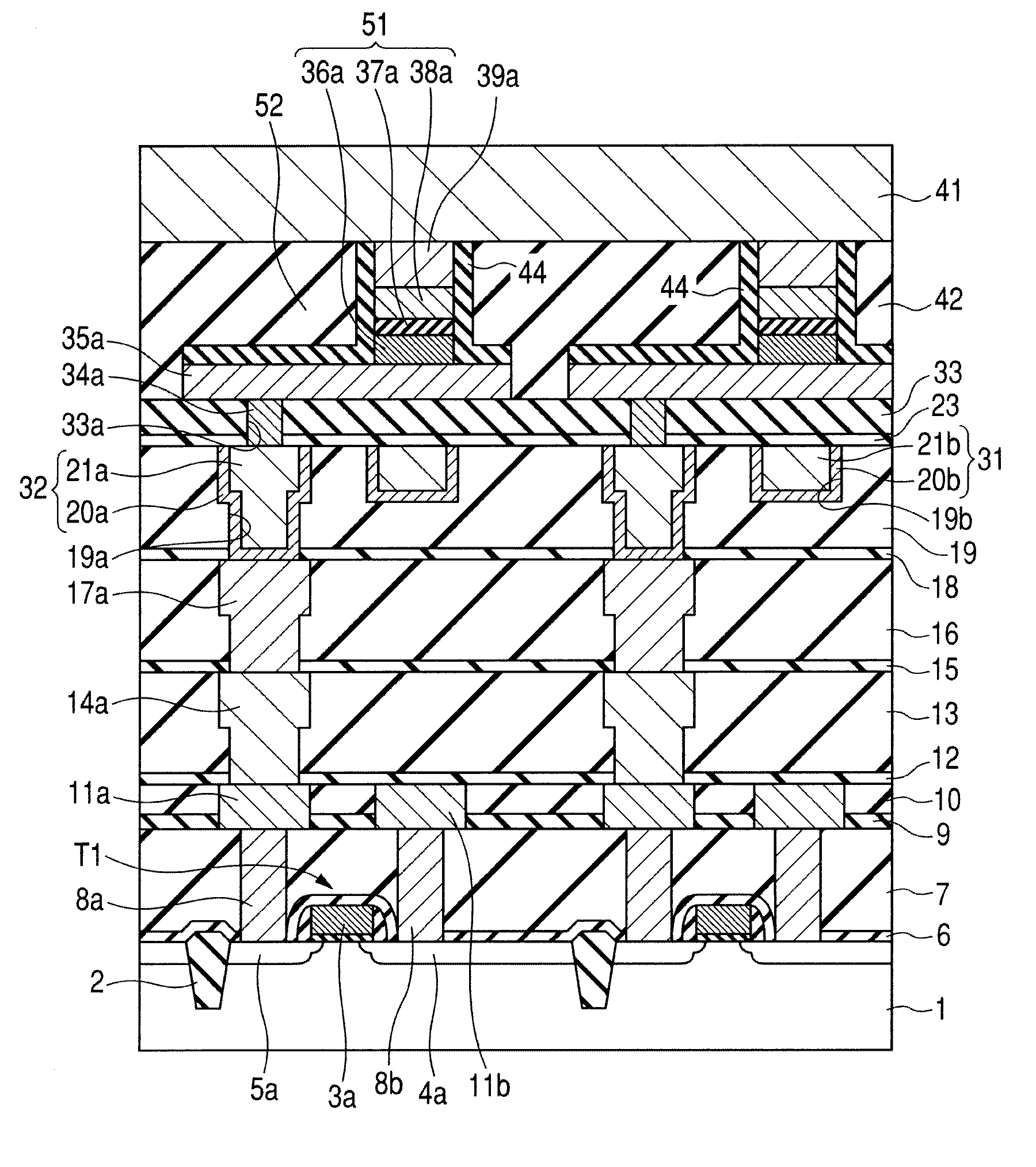
Figure 1 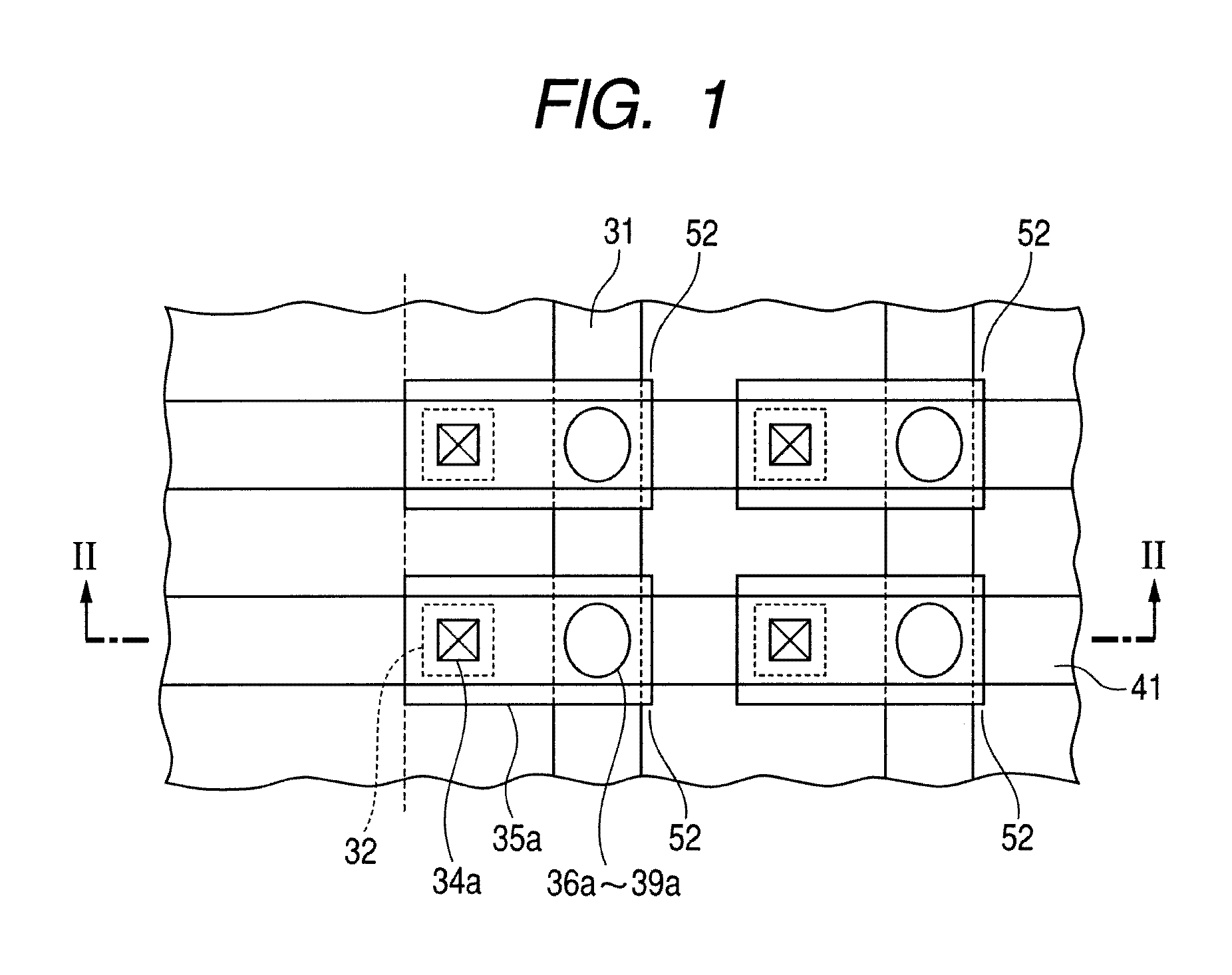
Figure 2 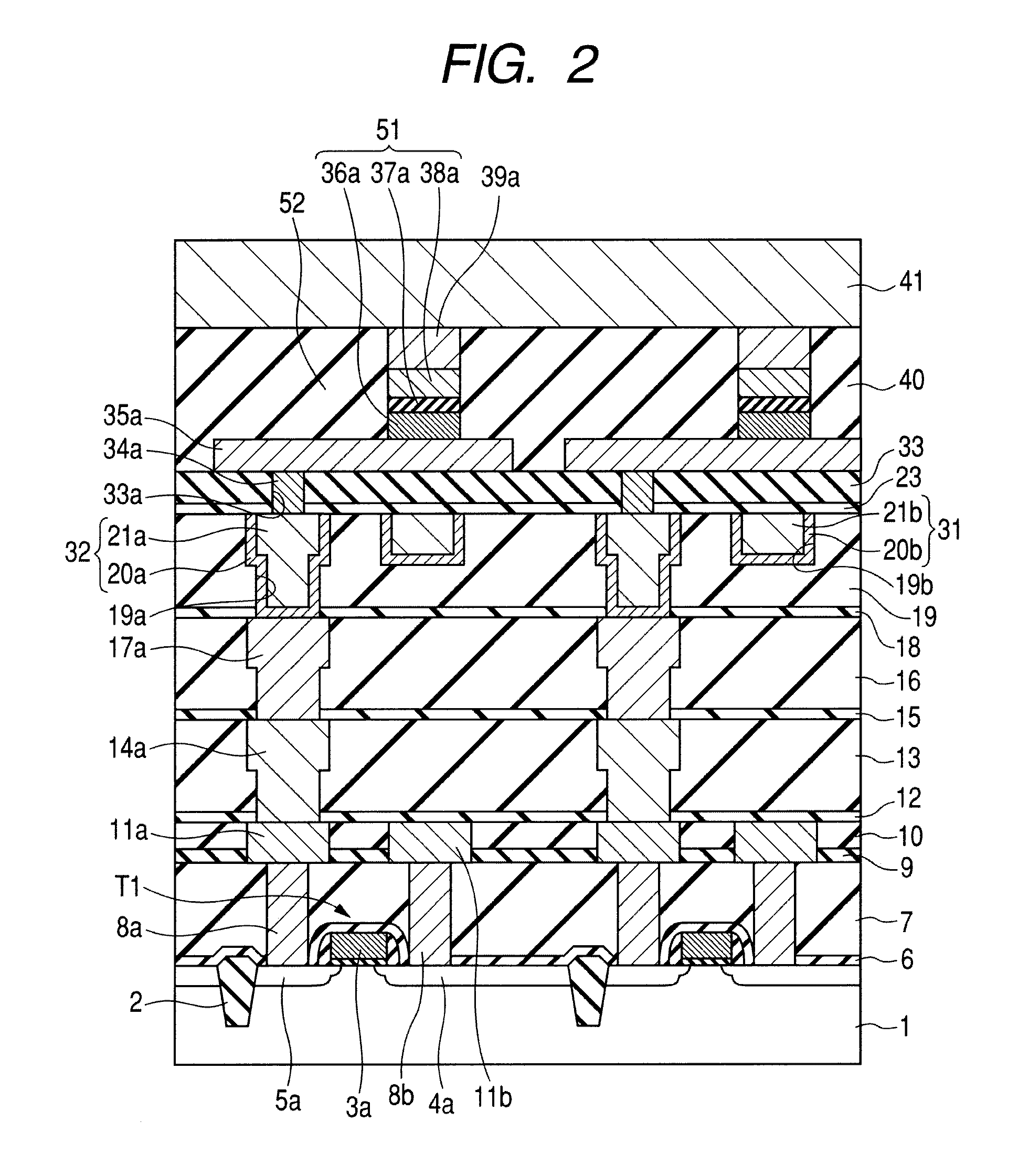
Figure 3
Abstract
Description
CROSS-REFERENCE TO RELATED APPLICATIONS
[0001] The disclosure of Japanese Patent Application No. 2009-198181 filed on Aug. 28, 2009 including the specification, drawings and abstract is incorporated herein by reference in its entirety.BACKGROUND OF THE INVENTION
[0002] The present invention relates to a semiconductor device and a method of manufacturing the same, and particularly to a semiconductor device including a magnetic resistor element and a method of manufacturing the same.
[0003] As a form of a semiconductor device, there is a Magnetic Random Access Memory (MRAM) to which a magnetic resistor element called a Magnetic Tunnel Junction (MTJ) is applied. In the MRAM, the magnetic resistor elements are formed in an array configuration. In each of the magnetic resistor elements, two magnetic layers are stacked with a tunnel insulating film interposed therebetween. According to whether magnetizations in the two magnetic layers are oriented into the same directions or into opposite direc...
Examples
embodiment 1
[0065]First, a description will be given to a structure of a memory cell region in a semiconductor device. As shown in FIG. 1, in a memory cell region M, a plurality of digit lines 31 are formed in mutually spaced-apart relation to extend in a direction, and a plurality of bit lines 41 are formed in mutually spaced-apart relation to extend in a direction substantially orthogonal to the direction. At the portions where the digit lines 31 and the bit lines 41 cross each other, magnetic resistor elements 51 are disposed. One ends of the magnetic resistor elements are coupled to the bit lines 41, while the other ends thereof are coupled to the drain regions of element selection transistors (not shown).
[0066]As shown in FIG. 2, each of the element selection transistors T1 has a gate electrode 3a, a source region 4a, and a drain region 5a, and is formed in a surface of an element formation region defined in a semiconductor substrate 1 by an isolation insulating film 2. An etching stopper ...
embodiment 2
[0123]Here, a description will be given to a technique in which the surface of the portion of the interlayer insulating film located in the memory cell region is set by etching at a position lower than that of the surface of the portion of the interlayer insulating film located in the peripheral region.
[0124]In the steps shown in FIG. 4 described above, the etching stopper film 23 is formed so as to cover the interlayer insulating film 19, and the interlayer insulating film 33 is formed over the etching stopper film 23. Then, as shown in FIG. 30, a resist pattern 71 is formed so as to expose the portion of the interlayer insulating film 33 located in the memory cell region M and cover the portion thereof located in the peripheral region P. Using the resist pattern 71 as a mask, the portion of the interlayer insulating film 33 located in the memory cell region M is etched to have the surface thereof set at a position lower than that of the surface of the portion of the interlayer ins...