
Manufacturing method of semiconductor device
A manufacturing method and semiconductor technology, applied in semiconductor/solid-state device manufacturing, electrical components, circuits, etc., can solve problems such as reducing the yield rate of semiconductor devices and affecting the performance of semiconductor devices, so as to prevent undercutting, improve performance, and avoid corrosion Effect
Patent Information
- Authority / Receiving Office
- CN · China
- Patent Type
- Patents(China)
- Current Assignee / Owner
- Publication Date
- 2020-04-07
Smart Images
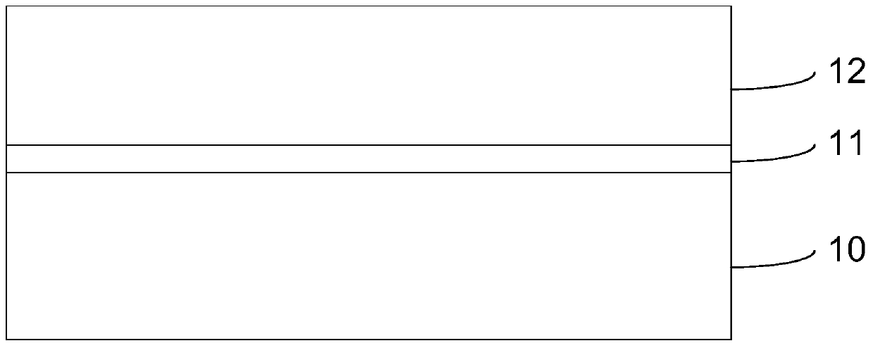
Figure 1 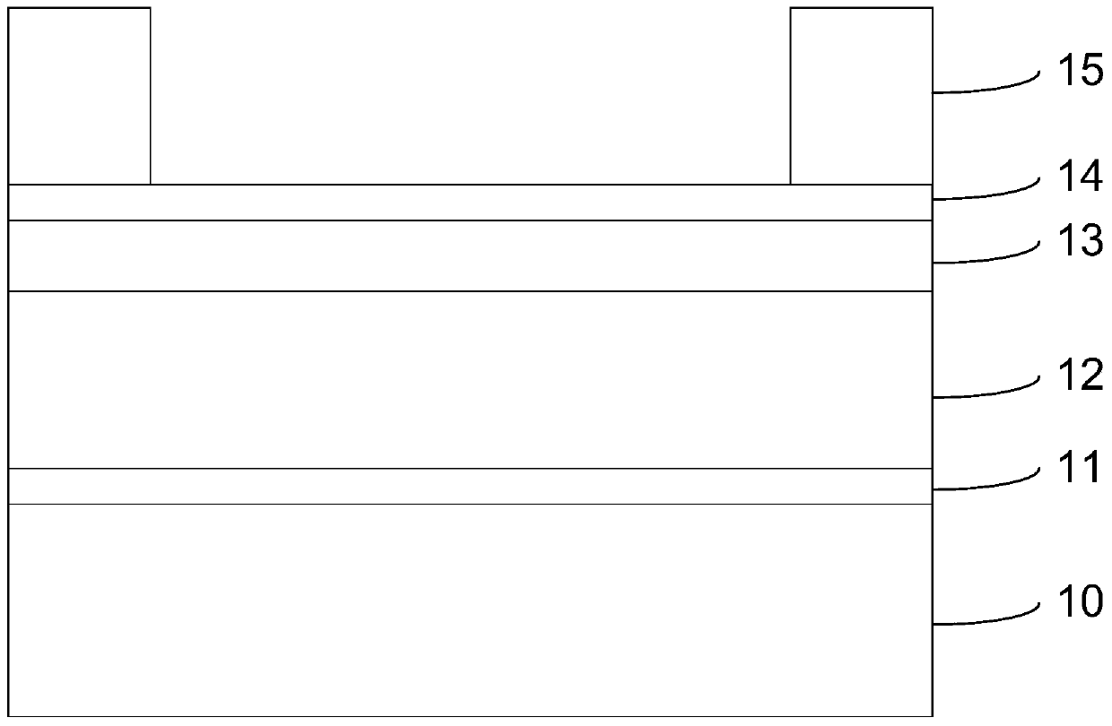
Figure 2 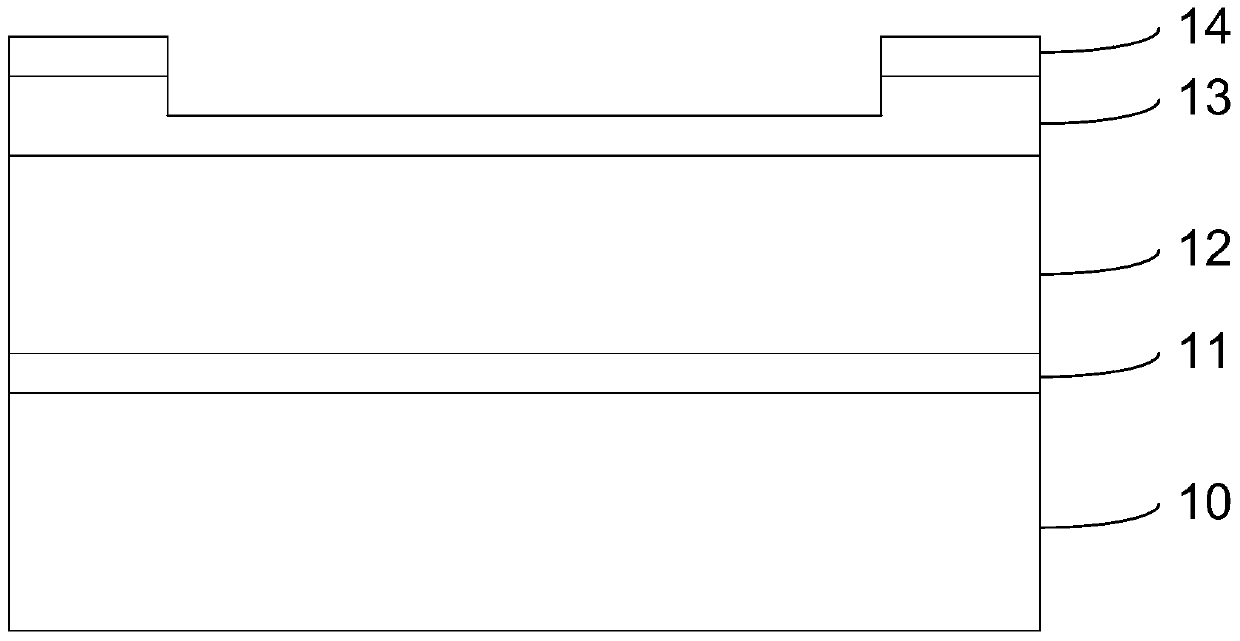
Figure 3
Abstract
Description
technical field
[0001] The invention relates to the technical field of semiconductors, in particular to a method for manufacturing a semiconductor device. Background technique
[0002] With the development of semiconductor technology, integrated circuits are developing in the direction of high integration. The requirement of high integration makes the line width of semiconductor devices smaller and smaller, and the reduction of line width puts forward higher requirements for the manufacturing process of integrated circuits.
[0003] Semiconductor devices are usually formed by multi-layer metal layers and multi-layer dielectric layers. The multi-layer metal layers are electrically connected by plugs arranged in the dielectric layers. As the line width decreases, the dielectric layer is now Dielectric materials with a low dielectric constant of less than 3 are often used.
[0004] In the prior art, after forming a low-k (dielectric constant less than 3) dielectric layer, a h...
Examples
Embodiment Construction
[0039] In order to make the content of the present invention clearer and easier to understand, the content of the present invention will be further described below in conjunction with the accompanying drawings. Of course, the present invention is not limited to this specific embodiment, and general replacements known to those skilled in the art are also covered within the protection scope of the present invention.
[0040] Secondly, the present invention is described in detail by means of schematic diagrams. When describing the examples of the present invention in detail, for the convenience of illustration, the schematic diagrams are not partially enlarged according to the general scale, which should not be used as a limitation of the present invention.
[0041] The structural diagram of each step of the manufacturing method of the semiconductor device well known to the inventor is as follows Figure 1~6 shown.
[0042] like figure 1 As shown, first a semiconductor substrat...