
A kind of manufacturing method of finfet device
A manufacturing method and device technology, applied in semiconductor/solid-state device manufacturing, semiconductor devices, electrical components, etc., can solve problems such as low sensitivity of threshold voltage, doping loss, etc., achieve improved lateral diffusion, achieve performance, and avoid outward diffusion Effect
Patent Information
- Authority / Receiving Office
- CN · China
- Patent Type
- Patents(China)
- Current Assignee / Owner
- Publication Date
- 2021-11-12
Smart Images
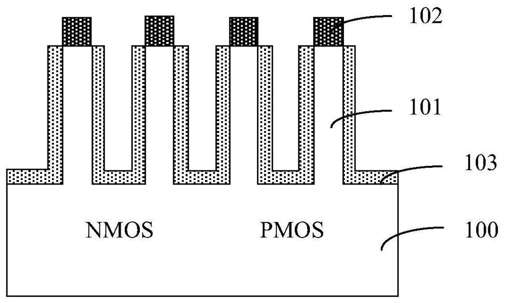
Figure 1 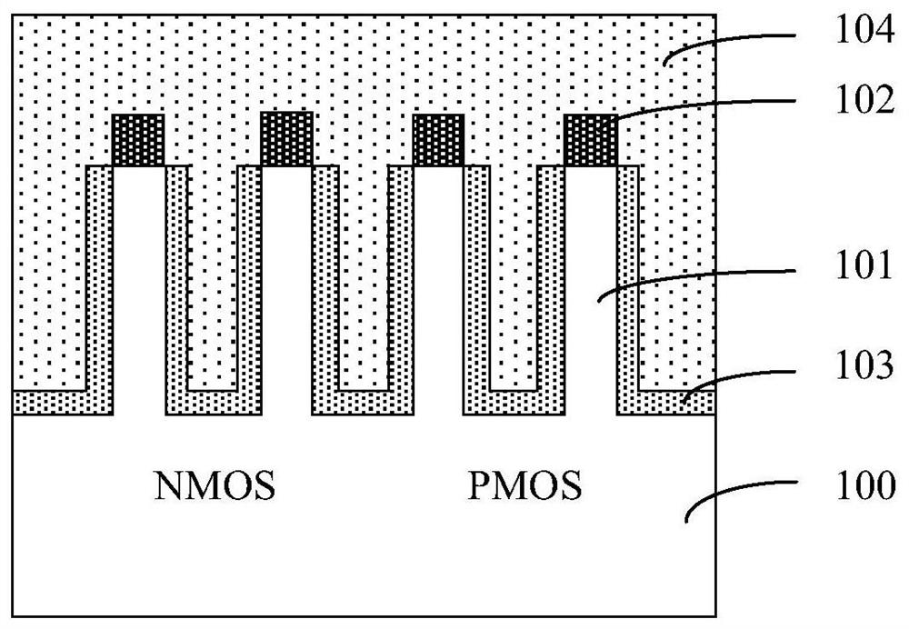
Figure 2 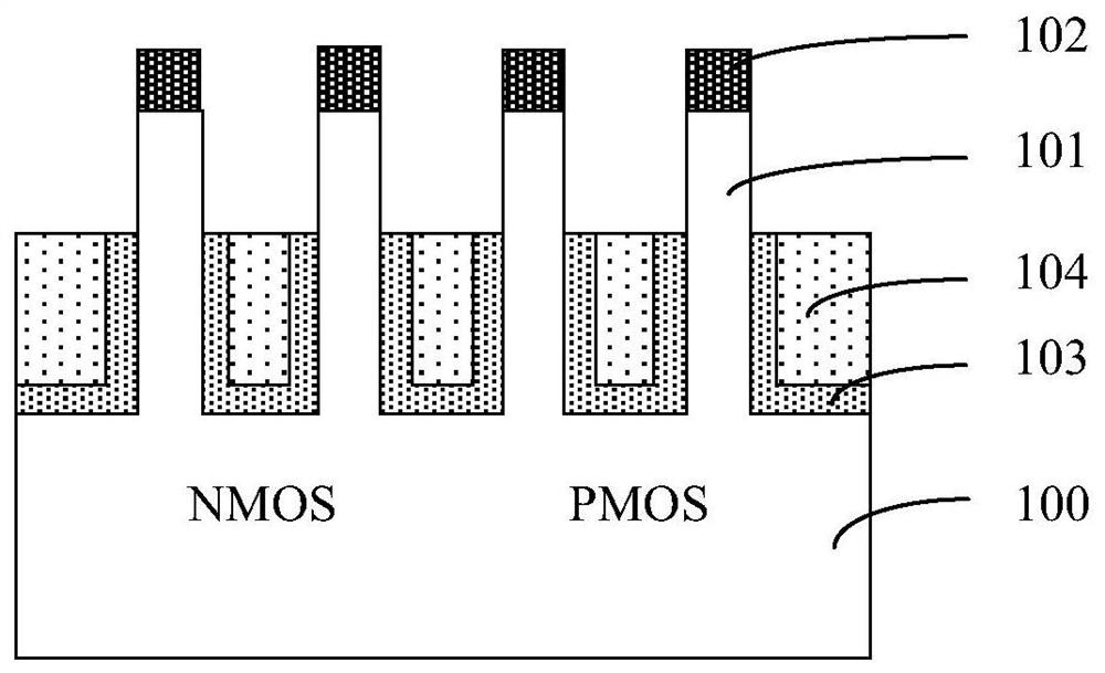
Figure 3
Abstract
Description
technical field
[0001] The invention relates to the technical field of semiconductors, in particular to a method for manufacturing a FinFET device. Background technique
[0002] With the continuous development of semiconductor technology, the improvement of integrated circuit (IC) performance is mainly achieved by continuously shrinking the size of integrated circuit devices to increase its speed. At present, due to the demand for high device density, high performance, and low cost, the semiconductor industry has advanced to the nanotechnology process node, and the fabrication of semiconductor devices is limited by various physical limits.
[0003] As the critical dimensions of semiconductor devices such as MOSFETs (Metal Oxide Semiconductor Field Effect Transistors) continue to shrink, short channel effects (SCE) are becoming more and more serious. Compared with existing planar transistors, FinFET (Fin Field Effect Transistor) has superior performance in terms of channel c...
Examples
Embodiment Construction
[0032] In the following description, numerous specific details are given in order to provide a more thorough understanding of the present invention. It will be apparent, however, to one skilled in the art that the present invention may be practiced without one or more of these details. In other examples, some technical features known in the art are not described in order to avoid confusion with the present invention.
[0033] It should be understood that the invention can be embodied in different forms and should not be construed as limited to the embodiments set forth herein. Rather, these embodiments are provided so that this disclosure will be thorough and complete, and will fully convey the scope of the invention to those skilled in the art. In the drawings, the size and relative sizes of layers and regions may be exaggerated for clarity. Like reference numerals refer to like elements throughout.
[0034] It will be understood that when an element or layer is referred t...