
Preparation method and product of a single-layer atomic channel fin field effect transistor
A fin-type field effect, transistor technology, applied in the field of applied research, to achieve the effects of good ohmic contact, strong gate control ability, and rich selectivity
Patent Information
- Authority / Receiving Office
- CN · China
- Patent Type
- Patents(China)
- Current Assignee / Owner
- Publication Date
- 2021-07-02
Smart Images
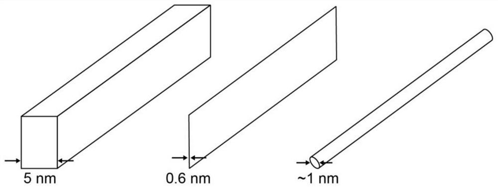
Figure 1 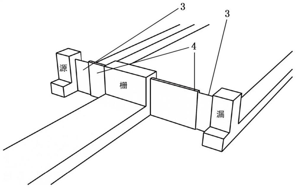
Figure 2 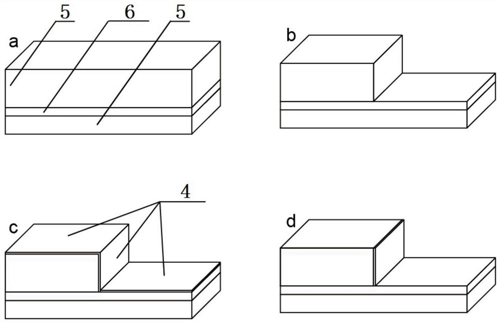
Figure 3
Abstract
Description
technical field
[0001] The invention belongs to the applied research field of nano artificial compound, micro-nano device, logic device, etc., and specifically provides a method for preparing a fin field-effect transistor of a single-atom-layer-thick channel material. Background technique
[0002] Moore's Law states that the number of transistors per unit area in an integrated circuit will double every year, which requires that the size of transistors be continuously reduced. When the channel width reaches below 10 nanometers, the quantum confinement effect of the traditional planar field effect transistor is significant, which hinders its further reduction in size. One of the solutions is to use a three-dimensional structure to construct a fin field effect transistor composed of a gate and a channel material covered by a dielectric layer. Thanks to the larger contact area between the gate and the channel material, and the thinner thickness of the channel material, the cont...
Examples
Embodiment 1
[0062] (1) SOI substrate of 300 nanometer silicon on the top layer (structural schematic diagram as image 3 Shown in a) The surface was spin-coated with LOR-7A (3K rpm, heated at 190°C, 5 minutes) and PMMA950K A7 (5K rpm, heated at 190°C, 5 minutes), and then exposed by electron beam exposure technology, and developed with Solution 1 (IPA / DI Water=1 / 3) was developed for 1 minute, developer 2 (CD-26) was developed for 35 seconds, and dried with nitrogen. Then use electron beam evaporation to deposit 200 nm thick metal nickel as a protective layer, and use inductively coupled plasma etching to remove the SOI top layer silicon material without metal protection, and finally dissolve the metal nickel with hydrochloric acid to obtain a vertical step pattern. The schematic diagram of the structure is as follows image 3 As shown in b, the actual enlarged picture is shown in Figure 4 shown;
[0063] (2) Use the atomic layer deposition method to deposit a uniform and dense hafnium ...
Embodiment 2
[0072] The difference from Example 1 is: the SOI substrate described in step (1) can be replaced with other substrates, such as a substrate with a similar SOI type three-layer structure, or a double-layer structure substrate, wherein the top layer can be Semiconductor, metal or insulator, the underlying material is an insulator.
[0073] Finfield-effect transistors with single-atom-layer-thick channel materials can be obtained.
Embodiment 3
[0075] The difference from Example 1 lies in that the thickness of the SOI top layer silicon in step (1) is different.
[0076] FinFETs with single-atom-layer-thick channel materials are available at different heights (up to microns).